
User Manual

CS4953xx Data Sheet
32-bit Audio Decoder DSP Family
DS705F2 10
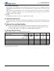
5.2 Recommended Operating Conditions
(GNDD = GNDIO = GNDA = 0 V; all voltages with respect to 0 V)
Note: It is recommended that the 3.3 V IO supply come up ahead of or simultaneously with the 1.8 V core supply.
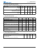
5.3 Digital DC Characteristics
(Measurements performed under static conditions.)
5.4 Power Supply Characteristics
(measurements performed under operating conditions)
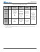
Parameter Symbol Min Typ Max Unit
DC power supplies: Core supply
PLL supply
I/O supply
|VDDA – VDDIO|
VDD
VDDA
VDDIO
1.71
3.13
3.13
1.8
3.3
3.3
0
1.89
3.46
3.46
V
V
V
V
Ambient operating temperature
Commercial Grade (CQZ/CVZ)
Automotive Grade (DQZ/DVZ)
T
A
0
- 40
+25
+25
+ 70
+ 85
°C
Commercial
Automotive
T
j
0
-40
—+125
+125
ºC
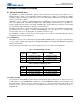
Parameter Symbol Min Typ Max Unit
High-level input voltage
V
IH
2.0 — — V
Low-level input voltage, except XTI
V
IL
——0.8 V
Low-level input voltage, XTI
V
ILXTI
——0.6 V
Input Hysteresis
V
hys
—0.4 — V
High-level output voltage (I
O
= -4mA), except XTI,
SDRAM pins
V
OH
VDDIO * 0.9 — — V
Low-level output voltage (I
O
= 4mA), except XTI, SDRAM
pins
V
OL
——VDDIO * 0.1V
SDRAM High-level output voltage (I
O
= -8mA)
V
OH
VDDIO * 0.9 — — V
SDRAM Low-level output voltage (I
O
= 8mA)
V
OL
——VDDIO * 0.1V
Input leakage current (all digital pins with internal pull-up
resistors disabled)
I
IN
—— 5 μA
Input leakage current (all digital pins with internal pull-up
resistors enabled, and XTI)
I
IN-PU
——70 μA
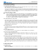
Parameter Min Typ Max Unit
Power supply current:
Core and I/O operating: VDD
1
PLL operating: VDDA
With external memory and most ports operating: VDDIO
1. Dependent on application firmware and DSP clock speed.
—
—
—
350
3.5
120
—
—
—
mA
mA
mA