
Manual

Pin Description
CS4953xx Hardware User’s Manual
DS732UM10 Copyright 2010 Cirrus Logic, Inc 9-11
memory). Insufficient grounding can degrade noise margins between devices resulting in data integrity
problems.
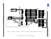
9.2.1.3 Decoupling
It is necessary to decouple the power supply by placing capacitors directly between the power and ground
of the CS4953xx. Each pair of power/ground pins (VDD1/GND1, etc.) should have its own decoupling
capacitor. The recommended procedure is to place a 0.1 uF capacitor as close as physically possible to
each power pin connected with a wide, low-inductance trace. A bulk capacitor of at least 10 uF is
recommended for each power plane.
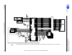
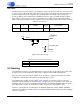
9.2.2 PLL Filter
9.2.2.1 Analog Power Conditioning
In order to obtain the best performance from the CS4953xx’s internal PLL, the analog power supply VDDA
must be as noise free as possible. A ferrite bead and two capacitors should be used to filter the VDDIO to
generate VDDA. This power scheme is shown in the Typical Connection diagrams.
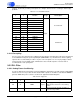
Table 9-3. Core and I/O Ground Pins
LQFP-144 Pin
#
LQFP-128 Pin
#
Pin Name Pin Type Pin Description
13 45 GND1
Input
Core Ground.
27 56 GND2
57 86 GND3
69 98 GND4
86 115 GND5
101 127 GND6
122 15 GND7
133 25 GND8
21 53 GNDIO1
I/O Ground
36 67 GNDIO2
47 76 GNDIO3
63 92 GNDIO4
76 105 GNDIO5
94 122 GNDIO6
116 9 GNDIO7
139 31 GNDIO8
Table 9-4. PLL Supply Pins
LQFP-144 Pin
#
LQFP-128 Pin
#
Pin Name Pin Type Pin Description
129 21 VDDA Input
PLL supply. This voltage must be 3.3V.
This must be clean, noise-free analog
power.
126 19 GNDA Input
PLL ground. This ground should be as
noise free as possible.