
Manual

Pin Description
CS4953xx Hardware User’s Manual
DS732UM10 Copyright 2010 Cirrus Logic, Inc 9-10
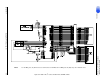
9.2 Pin Description
9.2.1 Power and Ground
The following sections describe the CS4953xx power and ground pins. Decoupling and conditioning of the
power supplies is also discussed. Following the recommendations for decoupling and power conditioning
will help to ensure reliable performance.
9.2.1.1 Power
The CS4953xx Family of DSPs take two supply voltages — the core supply voltage (VDD) and the I/O
supply voltage (VDDIO). There is also a separate analog supply voltage required for the internal PLL
(VDDA). These pins are described in the following tables and descriptions.
The DSP Core supply voltage pins require a nominal 1.8V. The DSP I/O supply voltage pins require a
nominal 3.3V.
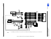
9.2.1.2 Ground
For two-layer circuit boards, care should be taken to have sufficient grounding between the DSP and parts
in which it will be interfacing (DACs, ADCs, S/PDIF Receivers, microcontrollers, and especially external
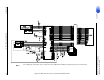
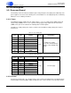
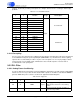
Table 9-1. Core Supply Pins
LQFP-144
Pin #
LQFP-128
Pin #
Pin Name Pin Type Pin Description
10 42 VDD1
Input
1.8V DSP Core supply.
This powers all internal logic
and the on-chip SRAMs and
ROMs
24 55 VDD2
54 83 VDD3
66 95 VDD4
83 112 VDD5
98 125 VDD6
119 12 VDD7
130 22 VDD8
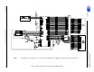
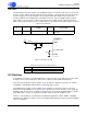
Table 9-2. I/O Supply Pins
LQFP-144
Pin #
LQFP-128
Pin #
Pin Name Pin Type Pin Description
18 50 VDDIO1
Input 3.3V I/O supply
33 62 VDDIO2
44 73 VDDIO3
60 89 VDDIO4
73 100 VDDIO5
91 120 VDDIO6
113 8 VDDIO7
136 28 VDDIO8