
Manual

Revision History
CS4953xx Hardware User’s Manual
DS732UM10 Copyright 2010 Cirrus Logic, Inc 9-29
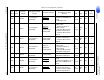
Revision History
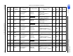
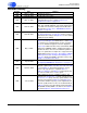
Revision Date Changes
UM1 MAY 17, 2006 Preliminary Release
UM2 AUG 24, 2006 Updated Boot Procedure
UM3 OCT 11, 2007
Updated CrusConfig register and corrected Output D1
and Input D2 messages. Update Section 2.5.2,
"Softboot Procedure" on page 2-15.
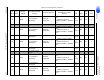
UM4 NOV 21, 2007
Added Bank Addressing note to Table 8-1 for SD_BA0/
EXT_A13 and SD_BA1/EXT_A14 signals. Added same
note with each schematic in Chapter 9. Modified Note
directly above Section 8.3.1, "SDRAM/Flash Interface
Signals" on page 8-2
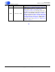
UM5 NOV 28, 2007
Changed definition for secondary functions in Section 9-
10 “Pin Assignments” on page 9-17 for pins 138 and
142. Made same changes in Figure 9-11 for the 144-Pin
LQFP pin layout drawing.
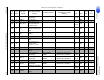
UM6 May 7, 2008
Changed text in Figure Titles for Figure 9-1, Figure 9-2,
Figure 9-4, and Figure 9-5. Modified Note 1 under Table
8-1. Change note regarding bank selection, in Figures
9-1 to 9-7. Added new typical connection diagram in
Figure 9-6, “LQFP-128, I
2
C Control, Serial FLASH, DSD
Audio Input, SDRAM, 7 DACs.” Modified description of
firmware modules offered on the CS4953xx platform on
page 1-3. Updated list of sample rates supported for the
Digital Audio Port in Section 6.1, "Description of Digital
Audio Input Port when Configured for DSD Input" on
page 6-1. Clarified availability of parallel control port in
Chapter 4, "Parallel Control Port".
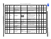
UM7 July 10, 2008
Added important notice a beginning of Section 8.3.2,
"Configuring SDRAM/Flash Parameters" on page 8-4.
UM8 April 23, 2009
Updated Figure 3-6, adding missing ACK timing
diagram. Updated Table 5-3, Table 5-4, Table 5-5. Table
5-6, and Table 7-4. Reformatted manual to current
Cirrus Logic style practices. Updated Table 3-1,
Table 3-2, Table 8-1 and Table 9-8, noting signals that
are active low with a line over the signal.
UM9 June 5, 2009
Added XTAL/2 frequency capability for Master and
Slave boot in Section 2.3.1.1.1.(Steps 5 and 8) and in
Section 2.3.2.1.1.(Steps 6 and 9). Updated Master and
Slave boot flow charts in Figure 2-2 and Figure 2-3 to
show where XTAL/2 frequency can be implemented if
desired. Updated values for A1, Left Justified 24-bit, in
Table 5-3. Removed overline which had designed Pins
SD_DQM0 and SD_DQM1 to be Active Low in Table 9-
10 and in Chapter 8, "External Memory Interfaces".