
Manual

DS732UM10 Copyright 2010 Cirrus Logic, Inc 9-27
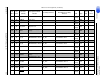
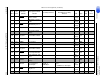
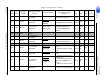
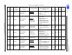
Pin Assignments
CS4953xx Hardware User’s Manual
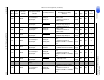
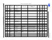
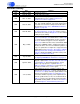
14 GPIO0
General Purpose
Input/Output
1. UART_CLK 1. UART Clock
3.3V
(5V tol)
BiDir IN Y
122 15 GNDD7 Core ground 0V PWR
123 16 XTAL_OUT
Buffered Reference
Clock Input/Crystal
Oscillator Input
3.3V
(5V tol)
OUT
124 17 XTI
Reference Clock
Input/Crystal Oscillator
Input
3.3V
(5V tol)
ANA
125 18 XTO
Crystal Oscillator
Output 1
3.3V ANA
126 19 GNDA PLL ground 1.8V PWR
127 - NC
Do Not Connect on
PCB
1.8V ANA
128 20
PLL_REF_RE
S
Current Reference
Output for PLL.
Connect to resistor.
3.3V ANA
129 21 VDDA PLL power. 3.3V PWR
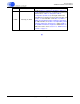
130 22 VDD8
Core power supply
voltage
1.8V PWR
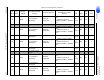
131 23 GPIO14
General Purpose
Input/Output
1. DAI1_DATA3
2. DSD3
1. PCM Audio Input Data 3
2. DSD Audio Input Data 3
3.3V
(5V tol)
BiDir IN Y
132 24 GPIO13
General Purpose
Input/Output
1. DAI1_DATA2
2. DSD2
1. PCM Audio Input Data 2
2. DSD Audio Input Data 2
3.3V
(5V tol)
BiDir IN Y
133 25 GNDD8 Core ground 0V PWR
134 26 GPIO12
General Purpose
Input/Output
1. DAI1_DATA1
2. DSD1
1. PCM Audio Input Data 1
2. DSD Audio Input Data 1
3.3V
(5V tol)
BiDir IN Y
135 27 DAI1_DATA0
PCM Audio Input Data
0
DSD0 DSD Audio Input Data 0
3.3V
(5V tol)
In Y
136 28 VDDIO8
I/O power supply
voltage
3.3V PWR
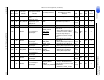
Table 9-10. Pin Assignments (Continued)
LQFP-
144
Pin #
LQFP-
128
Pin #
Function 1
(Default)
Description of Default
Function
Secondary Functions Description of Secondary
Functions
Pwr Type
Reset
State
Pullup
at
Reset