
Manual

Control
CS4953xx Hardware User’s Manual
DS732UM10 Copyright 2010 Cirrus Logic, Inc 9-14
Configuration and control of the CS4953xx decoder and its peripherals are indirectly executed through a
messaging protocol supported by the operating system (O/S) running on the DSP. In other words,
successful communication can only be accomplished by following the low-level hardware communication
format and high-level messaging protocol. The specifications of the messaging protocol used by the O/S
can be found in AN288, “CS4953xx/Cs497xxx Firmware User’s Manual”. The system designer only needs
to read the subsection describing the communication mode being used. The CS4953xx Hardware User’s
Manual explains each communication mode in more detail.
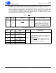
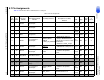
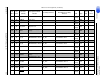
Table 9-8. Reset Pin
LQFP-144
Pin #
LQFP-128
Pin #
Pin Name Pin Type Pin Description
93 121 RESET Input
Reset, async. active-low Chip Reset
Reset should be low at power-up to
initialize the DSP and to guarantee
that the device is not active during
initial power-on stabilization periods.
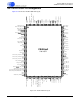
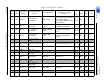
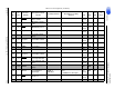
Table 9-9. Hardware Strap Pins
LQFP-144
Pin #
LQFP-128
Pin #
Pin Name Pin Type Pin Description
739
DAO2_DATA1, HS4,
GPIO19
Input
Operational Mode Select
Pull-up or Pull-down resistors on these pins set
the DSP operational mode at reset. Hardware
Strap Mode Select
The state of these pins is latched at the rising
edge of
RESET. The boot ROM uses the state of
these pins to select the boot mode.
11 43
DAO2_DATA0, HS3,
GPIO18
16 48
DAO1_DATA2, HS2,
GPIO16
17 49
DAO1_DATA1, HS1,
GPIO15
19 51 DAO1_DATA0, HS0