
Manual

Control
CS4953xx Hardware User’s Manual
DS732UM10 Copyright 2010 Cirrus Logic, Inc 9-13
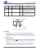
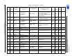
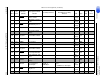
Figure 9-10. Crystal Oscillator Circuit Diagram
9.4 Control
The CS4953xx supports 5 control interface protocols: SPI, I
2
C, Motorola parallel, Intel parallel, and
Multiplexed Intel parallel mode. All slave serial control modes between the DSP and the host
microcontroller use the Serial Control Port 1 (SCP1) pins. Parallel slave control modes are implemented
on the Parallel Control Port (PCP) pins. A second serial control port (SCP2) is available for master mode
applications.
9.4.1 Operational Mode
The control interface protocol used is determined by the state of the Hardware Strap pins, HS[4:0] which
are sampled at the rising edge of RESET
. The HS[4:0] pins should be pulled to VDD or GND using 10 kΩ
resistors according to the specific control mode desired as shown in Table 2-1, "Operation Modes" on
page 2-3.
The following sections describe the pins used for the 5 control modes. For example diagrams of system
connection, please see Section 9.1, "Typical Connection Diagrams" on page 9-1. For information on
timing diagrams and messaging protocol to the CS4953xx, see Chapter 2, "Operational Modes".
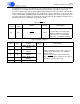
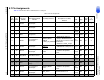
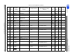
Table 9-7. DSP Core Clock Pins
LQFP-144 Pin
#
LQFP-128 Pin
#
Pin Name Pin Type Pin Description
123 16 XTAL_OUT Output Buffered version of XTI.
124 17 XTI Input
Reference Clock Input/Crystal Oscillator
Input. An external clock may be input
directly to this pin or one end of a crystal
may be connected to this pin.
125 18 XTO Output
Crystal Oscillator Output. One end of a
crystal oscillator is connected to this pin.
This pin cannot be used to drive external
circuitry.
1 Meg
C1 C1
X1
XTI
XTO
XTAL_OUT
To System
CS4953x
x