CS4953xx 32-bit Audio DSP Family CS4953xx H ardwa re Us er ’s Manual Preliminary Product Information This document contains information for a new product. Cirrus Logic reserves the right to modify this product without notice. Copyright 2010 Cirrus Logic, Inc. http://www.cirrus.
CS4953xx Hardware User’s Manual Contacting Cirrus Logic Support For all product questions and inquiries contact a Cirrus Logic Sales Representative. To find the one nearest to you go to www.cirrus.com IMPORTANT NOTICE “Preliminary” product information describes products that are in production, but for which full characterization data is not yet available. Cirrus Logic, Inc. and its subsidiaries (“Cirrus”) believe that the information contained in this document is accurate and reliable.
Contents CS4953xx Hardware User’s Manual Contents Contents . . . . . . . . . . . . . . . . . . . . . . . . . . . . . . . . . . . . . . . . . . . . . . . . . . . . . . . . . . . . . . . . . . . . . . . iii Figures . . . . . . . . . . . . . . . . . . . . . . . . . . . . . . . . . . . . . . . . . . . . . . . . . . . . . . . . . . . . . . . . . . . . . . . . v Tables . . . . . . . . . . . . . . . . . . . . . . . . . . . . . . . . . . . . . . . . . . . . . . . . . . . . . . . . . . . . . . . . . . . . . . . .
Contents CS4953xx Hardware User’s Manual 3.2 Serial Control Port Configuration. . . . . . . . . . . . . . . . . . . . . . . . . . . . . . . . . . . . . . . . . . . . . . .3-1 3.3 I2C Port . . . . . . . . . . . . . . . . . . . . . . . . . . . . . . . . . . . . . . . . . . . . . . . . . . . . . . . . . . . . . . . . . . . .3-2 3.3.1 I2C System Bus Description ...........................................................................................3-2 3.3.2 I2C Bus Dynamics .................................
Figures CS4953xx Hardware User’s Manual Chapter 8. External Memory Interfaces ............................................................... 8-1 8.1 SDRAM Controller . . . . . . . . . . . . . . . . . . . . . . . . . . . . . . . . . . . . . . . . . . . . . . . . . . . . . . . . . . .8-1 8.2 Flash Memory Controller. . . . . . . . . . . . . . . . . . . . . . . . . . . . . . . . . . . . . . . . . . . . . . . . . . . . . .8-2 8.2.1 Flash Controller Interface ....................................................
Figures CS4953xx Hardware User’s Manual Figure 3-8. I2C Write Flow Diagram ..............................................................................................................3-8 Figure 3-9. I2C Read Flow Diagram ............................................................................................................3-10 Figure 3-10. Sample Waveform for I2C Write Functional TIming ................................................................3-12 Figure 3-11.
Tables CS4953xx Hardware User’s Manual Tables Table 2-1. Operation Modes..........................................................................................................................2-3 Table 2-2. SLAVE_BOOT message for CS4953xx .....................................................................................2-10 Table 2-3. HCMB_PARALLEL Message for CS4953xx ..............................................................................2-10 Table 2-4. HCMB_I2C message for the CS4953xx.......
CS4953xx Hardware User’s Manual Table 9-4. PLL Supply Pins.........................................................................................................................9-11 Table 9-5. PLL Filter Pins............................................................................................................................9-12 Table 9-6. Reference PLL Component Values............................................................................................9-12 Table 9-7. DSP Core Clock Pins ...
Overview CS4953xx Hardware User’s Manual Chapter 1 Introduction 1.1 Overview The CS4953xx is a programmable audio DSP that combines a programmable, 32-bit fixed-point general purpose DSP with dedicated audio peripherals. Its audio-centric interfaces facilitate the coding of highprecision audio applications and provide a seamless connection to external audio peripheral ICs. The CS4953xx is a 32-bit RAM-based processor that provides up to 150 MIPS of processing power and includes all standard codes in ROM.
Overview CS4953xx Hardware User’s Manual Figure 1-1 illustrates the functional block diagram for the CS4953xx chip.
Functional Overview of the CS4953xx Chip CS4953xx Hardware User’s Manual 1.2 Functional Overview of the CS4953xx Chip The CS4953xx chip supports a maximum clock speed of 150 MHz in a 144-pin LQFP or 128-pin LQFP package. A high-level functional description of the CS4953xx chip is provided in this section. 1.2.
Functional Overview of the CS4953xx Chip CS4953xx Hardware User’s Manual 1.2.6 Compressed Data Input / Digital Audio Input (DAI2) Controller The DAI2 controller has one input port and its own SCLK and LRCLK and can be used for accepting PCM data in the same way as DAI1, but is used primarily for the delivery of compressed data.
Functional Overview of the CS4953xx Chip CS4953xx Hardware User’s Manual By default, SCP2 is configured as a master to access a serial FLASH/EEPROM for either booting the DSP or retrieving configuration information. As a master, it can drive the clock signal at up to 1/2 of the DSP’s core clock speed. The CS4953xx has two additional serial communication pins not specified in either the I2C or SPI specification. The port uses the SCP1_IRQ pin to indicate that a read message is ready for the host.
Functional Overview of the CS4953xx Chip CS4953xx Hardware User’s Manual 1.2.15 Clock Manager and PLL The CS4953xx Clock Manager and PLL module contains an Analog PLL, RTL Clock Synthesizer, and Clock Manager. The Analog PLL is a customized analog hard macro that contains the Phase Detector (PD), Charge Pump, Loop Filter, VCO, and other non-digital PLL logic. The Clock Synthesizer is a digital design wrapper around the analog PLL that allows clock frequency ranges to be programmed.
Overview CS4953xx Hardware User’s Manual Chapter 2 Operational Modes 2.1 Overview The CS4953xx has several operational modes that can be used to conform to many system configurations. The operational modes for the CS4953xx specify both the communication mode and boot mode. This chapter discusses the selection of operational modes, booting procedures and performing a soft reset. The CS4953xx can be either a slave device or a master device for the boot procedure.
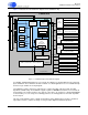
Overview CS4953xx Hardware User’s Manual P a ra lle l M e m o ry B u s / SCP2 C o n tro l B u s S y s te m H o s t C o n tro lle r (M a s te r) E x te rn a l R O M / E x t.
Operational Mode Selection CS4953xx Hardware User’s Manual 2.2 Operational Mode Selection The operational mode for the CS4953xx is selected by the values of the HS[4:0] pins on the rising edge of RESET. This value determines the communication mode used until the part is reset again. This value also determines the method for loading application code. The table below shows the different operational modes and the HS[4:0] values for each mode. Table 2-1.
Slave Boot Procedures CS4953xx Hardware User’s Manual 2.3 Slave Boot Procedures When the CS4953xx is the slave boot device, the system host controller (as the master boot device) must follow an outlined procedure for correctly loading application code. The two methods of slave boot for the CS4953xx, slave boot and host-controlled master boot are described in this section. Each of these methods requires the system host controller to send messages to, and read back messages from, the CS4953xx.
Slave Boot Procedures CS4953xx Hardware User’s Manual 2.3.1.1 Performing a Host Controlled Master Boot (HCMB) Figure 2-2 shows the steps taken during a Host Controlled Master Boot (HCMB). The procedure is discussed in Section 2.3.1.1.1.
Slave Boot Procedures CS4953xx Hardware User’s Manual 3. Wait for 10 μS. 4. Read the BOOT_START message (See NOTE 1 in Figure 2-2). If the initialization is successful, CS4953xx sends out the BOOT_START message and the host proceeds to Step 6. If initialization fails, the host must return to Step 1, and if failure is met again, the communication timing and protocol should be inspected. 5. The host sends the boot assist BOOT_ASSIST_A.uld file or boot_assist_xtal_div2_a*.
Slave Boot Procedures CS4953xx Hardware User’s Manual 17. Read the APP_START message. If code execution is successful, the CS4953xx sends out an APP_START message. This indicates that the code has been initialized and can accept further configuration messages. The host should not attempt further communication with the CS4953xx until the APP_START message has been read. If the CS4953xx does not send an application start message, the host must return to Step 1. 18. Send Hardware Configuration messages.
Slave Boot Procedures CS4953xx Hardware User’s Manual 2.3.2.1 Performing a Slave Boot Figure 2-3 shows the steps taken during a Slave boot. The procedure is discussed in Section 2.3.2.1.1.. START WRITE_*(SLAVE_BOOT) RESET# (LOW) READ_*(MSG)NOTE 2 SET HS[3:0] PINS FOR OPERATIONAL MODE MSG ==BOOT_START RESET# (HIGH) N EXIT (ERROR) Y WAIT 50 μS WRITE_*(.
Slave Boot Procedures CS4953xx Hardware User’s Manual 3. Send the SLAVE_BOOT message. The host sends the appropriate SLAVE_BOOT message to the CS4953xx using the control port specified (serial port/parallel port) and format specified (I2C, SPI, Intel, etc.) by the HS[4:0] pins at reset. 4. Wait for 10 μS. 5. Read the BOOT_START message (See NOTE 1 in Figure 2-3). If the initialization is successful, CS4953xx sends out the BOOT_START message and the host proceeds to Step 6.
Slave Boot Procedures CS4953xx Hardware User’s Manual APP_START message. This indicates that the code has been initialized and can accept further configuration messages. The host should not attempt further communication with the CS4953xx until the APP_START message has been read. If the CS4953xx does not send an application start message, the host must return to Step 1. 20. Send Hardware Configuration messages. The slave boot procedure is completed.
Slave Boot Procedures CS4953xx Hardware User’s Manual HCMB_PARALLEL is used when the application code is stored in external parallel ROM, such as an external 8-bit or 16-bit EEPROM or Flash. The external data bus width is specified by the ‘M’ variable in the first control word. Also, the 20-bit start address is specified in the second control word with the ‘A’ variable. Read cycle parameters can also be configured by the ‘x’ and ‘y’ variables.
Slave Boot Procedures CS4953xx Hardware User’s Manual The SPI clock is derived from the internal core clock. This clock can be divided down with the “c” 12-bit divider variable. The command byte (the first byte to the SPI ROM) can be defined by the “s” variable. The CS4953xx control port used for the HCMB_SPI can be configured by the ‘p’ variable. Finally, the “S” variable configures the chip select used, according to Table 2-6 below. Table 2-6.
Master Boot Procedure CS4953xx Hardware User’s Manual Table 2-9 is a quick reference showing the different boot commands understood by the CS4953xx, in mnemonic and actual hex value, used in CS4953xx boot sequences. Table 2-9. Boot Command Messages for CS4953xx MNEMONIC VALUE DETAILED TABLE SLAVE_BOOT 0x8000 0000 Table 2-2 HCMB_PARALLEL 0xE0== ==== Table 2-3 HCMB_I2C 0xC0== ==== Table 2-4 HCMB_SPI 0xD=== ==== Table 2-5 SOFT_RESET 0x40 00 00 00 Table 2-7 2.
Softboot CS4953xx Hardware User’s Manual 2.5 Softboot The O/S application code for the CS4953xx allows users to swap out one or more overlays during run time, without the need for re-download of the entire overlay stack. This is helpful for reducing the time required for switching between different types of incoming audio data streams.
Softboot CS4953xx Hardware User’s Manual 2.5.2 Softboot Procedure Figure 2-5 contains a flow diagram and description of the Softboot procedure. This is a step-by-step guideline that can be used as an aid in developing the system controller code required to drive the CS4953xx. START WRITE_* (SOFTBOOT) N IRQ == LOW? Y READ_* (MSG) N N TIMEOUT? Y EXIT(ERROR) MSG == SOFTBOOT_ACK? GO TO STEP 10, Section 2.5.2.3. Y LOAD OVERLAYS DONE Figure 2-5. Soft Boot Sequence Flowchart 2.5.2.
Softboot CS4953xx Hardware User’s Manual 2.5.2.2 Softboot Example Figure 2-6 contains an example softboot flow diagram. Section 2.5.2.3.provides a step-by-step description of the Softboot procedure using the Host Control Master Boot (HCMB) procedure that is most commonly used CS4593x systems.
Softboot CS4953xx Hardware User’s Manual 2.5.2.3 Softboot Example Steps 1. Send the SOFTBOOT message. The host sends the SOFTBOOT message to the CS4953xx to begin overlay swap. 2. Wait for IRQ low. The host then waits for SCP1_IRQ (or PCP_IRQ) to go low. If the TIMEOUT period has been reached, the host should exit. If the IRQ pin is LOW, proceed to Step 3. 3. Read the SOFTBOOT_ACK message. If the message is the SOFTBOOT_ACK message (0x00000005), then the host should proceed to Step 4.
Softboot CS4953xx Hardware User’s Manual §§ DS732UM10 Copyright 2010 Cirrus Logic, Inc 2-18
Overview CS4953xx Hardware User’s Manual Chapter 3 Serial Control Port 3.1 Overview The CS4953xx uses the Serial Control Port (SCP) to communicate with external devices such as host microprocessors using either I2C or SPI serial communication formats. Each port can be configured as either a master or slave. The CS4953xx DSP serial port communicates using the SCP_CLK, SCP_MOSI, and SCP_MISO (SPI serial master and slave modes), and SCP_SDA (for I2C serial master and slave modes) pins.
I2C Port CS4953xx Hardware User’s Manual 3.3 I2C Port The CS4953xx I2C bus has been developed for 8-bit digital control applications, such as those requiring microcontrollers. The I2C bus interface is a bidirectional serial port that uses 2 lines (data and clock) for data transmission and reception with software-addressable external devices.
I2C Port CS4953xx Hardware User’s Manual As seen in Figure 3-2, two serial ports are available on the CS4953xx. Each can be configured as either master or slave. For Audio applications, SCP1 is configured as a slave port and SCP2 is configured as a master port. SCP2 is used only in systems that are booting from serial EEPROM. 3.3V 3.3k 3.3k 3.3k CS4953xx RESET SCP1_CLK SCP1_SDA SCP1_IRQ SCP1_BSY System Microcontroller SLAVE ONLY 3.3k 3.3V 3.3k EEPROM Serial Clock Serial Data 3.
I2C Port CS4953xx Hardware User’s Manual Table 3-1. Serial Control Port 1 I2C Signals (Continued) Pin Name Pin Description LQFP-144 Pin # LQFP-128 Pin # Pin Type SCP2_CLK I2C Control Port Bit Clock. In master mode, this pin serves as the serial control clock output (open drain in I2C mode / output in SPI mode). In serial slave mode, this pin serves as the serial control clock input. In I2C slave mode the clock can be pulled low by the port to stall the master.
I2C Port CS4953xx Hardware User’s Manual The number of bytes that can be transmitted per transfer is unrestricted. Data is transferred with the mostsignificant bit (MSB) first. The first byte is an address byte that is always sent by the master after a Start or repeated Start condition. This byte must be a 7-bit I2C slave address + R/W bit. The 7-bit I2C address for the CS4953xx is 1000000b (0x80).
I2C Port CS4953xx Hardware User’s Manual Start SCP1_CLK SCP1_SDA A[6] A[5] A[4] A[3] A[2] A[1] A[0] R/W ACK Data Byte ACK Write M S M S Read M S S M Data Byte NACK Start SCP1_CLK SCP1_SDA A[6] A[5] A[4] A[3] A[2] A[1] A[0] R/W ACK Write M S M S Read M S S M M = Master Drives SDA S = Slave Drives SDA Figure 3-5.
I2C Port CS4953xx Hardware User’s Manual Stop SCP1_CLK SCP1_SDA Data Byte ACK Write M S M Read S M M Stop SCP1_CLK SCP1_SDA Data Byte NACK Write M S M M M S M = Master Drives SDA S = Slave Drives SDA Read Figure 3-7. Stop Condition with ACK and NACK If a slave cannot receive or transmit another complete byte of data until it has performed some other function, for example servicing an internal interrupt, it can hold the SCP1_CLK line low to force the master into a wait state.
I2C Port CS4953xx Hardware User’s Manual 3.3.3.2 Performing a Serial I2C Write Information provided in this section is intended as a functional description indicating how to use the configured serial control port to perform a I2C write from an external device (master) to the CS4953xx DSP (slave). The system designer must ensure that all timing constraints of the I2C write cycle are met (see the CS4953xx datasheet for timing specifications).
I2C Port CS4953xx Hardware User’s Manual 3.3.3.3 I2C Write Protocol 1. An I2C transfer is initiated with an I2C start condition which is defined as the data (SCP1_SDA) line falling while the clock (SCP1_CLK) is held high. 2. This is followed by a 7-bit address and the read/write bit held low for a write. So, the master should send 0x80. The 0x80 byte represents the 7-bit I2C address 1000000b, and the least significant bit set to ‘0’, designates a write. 3.
I2C Port CS4953xx Hardware User’s Manual START N SCP1_IRQ (LOW)? Y SEND I2C START: DRIVE SCP1_SDA LOW WHILE SCP1_CLK IS HIGH WRITE ADDRESS BYTE 0x81 N EXIT (ERROR) SCP1_SDA == ACK? Y READ DATA BYTE SEND ACK BYTES READ = 4? N Y SCP1_IRQ LOW? Y N SEND NACK SEND I2C STOP: DRIVE SCP1_SDA HIGH WHILE SCP1_CLK IS HIGH Figure 3-9.
I2C Port CS4953xx Hardware User’s Manual 3.3.3.5 I2C Read Procedure 1. An I2C read transaction is initiated by CS4953xx driving SCP1_IRQ low, signaling that it has data to be read. 2. The master responds by sending an I2C Start condition which is SCP1_SDA going low while SCP1_CLK is held high. 3. This is followed by a 7-bit address and the read/write bit set high for a read. So, the master should send 0x81.
Stop M S M S M S M S M K Data Byte 0 (LSB) AC K Data Byte 1 AC Data Byte 2 AC Data Byte 3 (MSB) K 7-bit Address AC SCP1_SDA K SCP1_CLK R /W AC K DS732UM10 Start S M 1. The I2C slave is always responsible for driving the ACK for the address byte. Notes: 2. The I2C slave is responsible for driving the ACK during I2C writes. Figure 3-10.
SPI Port CS4953xx Hardware User’s Manual 3.3.3.6 SCP1_IRQ Behavior Once the BOOT_ASSIST_A (.ULD file) has been downloaded in accordance to Steps 1 through 8 in Section 2.3.1 “Host Controlled Master Boot” on page 4 or Steps 1 through 8 in Section 2.3.2 “Slave Boot” on page 7, the SCP1_IRQ pin is functionally enabled. The SCP1_IRQ signal is not part of the I2C protocol, but is provided so that the slave can signal that it has data to be read.
SPI Port CS4953xx Hardware User’s Manual Table 3-2 shows the signal names, descriptions, and pin number of the signals associated with the SPI Serial Control Port on the CS4953xx. Table 3-2. Serial Control Port SPI Signals Pin Name Pin Description LQFP-144 Pin # LQFP-128 Pin # Pin Type SCP1_CS SPI Chip Select, Active Low In serial SPI slave mode, this pin is used as the active-low chipselect input signal.
SPI Port CS4953xx Hardware User’s Manual Table 3-2. Serial Control Port SPI Signals (Continued) Pin Name Pin Description LQFP-144 Pin # LQFP-128 Pin # Pin Type SCP2_IRQ Serial Control Port Data Ready Interrupt Request Output, Active Low This pin is driven low when the DSP has a message for the host to read. The pin will go high when the host has read the message and the DSP has no further messages. This pin reflects the state of the SCP1 port Transmit Buffer Empty Flag. 108 5 Open Drain 3.4.
SPI Port CS4953xx Hardware User’s Manual The data bits of the SCP1_MOSI and SCP1_MISO line are valid on the rising edge of SCP1_CLK. It is the slave’s responsibility to accept or supply bytes on the bus at the rate at which the master is driving SCP1_CLK. All data put on the SCP1_MOSI and SCP1_MISO lines must be in 8-bit bytes. The number of bytes that can be transmitted per transfer is unrestricted. Data is transferred with the most-significant bit (MSB) first.
SPI Port CS4953xx Hardware User’s Manual 3.4.3.1 Performing a Serial SPI Write Information provided in this section is intended as a functional description indicating how to perform an SPI write from an external device (master) to the CS4953xx DSP (slave). The system designer must ensure that all timing constraints of the SPI Write Cycle are met (see the CS4953xx datasheet for timing specifications).
SPI Port CS4953xx Hardware User’s Manual 5. The master should poll the SCP1_BSY signal until it goes high. If the SCP1_BSY signal is low, it indicates that the CS4953xx is busy performing some task that requires halting the serial control port. Once the CS4953xx is able to receive more data words, the SCP1_BSY signal will go high. Once the SCP1_BSY signal is high, proceed to Step 3. 6. The master finishes the SPI write transaction by driving the CS4953xx SCP1_CS signal high. 3.4.3.
SPI Port CS4953xx Hardware User’s Manual 3.4.3.4 SPI Read Protocol 1. An SPI read transaction is initiated by the CS4953xx slave driving SCP1_IRQ low to indicate that it has data to be read. 2. The master begins a SPI transaction driving chip select (SCP1_CS) low. 3. This is followed by a 7-bit address and the read/write bit set high for a read. So, the master should send 0x81. The 0x81 byte represents the 7-bit SPI address 1000000b, and the least significant bit set to ‘1’, designates a read. 4.
DS732UM10 SCP1_CS SCP1_MOSI 7-bit Address R/ W SCP1_CLK Data Byte 3 (MSB) Data Byte 2 Data Byte 1 Data Byte 0 (LSB) Figure 3-17. Sample Waveform for SPI Write Functional Timing Copyright 2010 Cirrus Logic, Inc SCP1_CS SCP1_MOSI SCP1_MISO 7-bit Address R /W SCP1_CLK Data Byte 3 (MSB) Data Byte 2 Data Byte 1 Data Byte 0 (LS SCP1_IRQ Figure 3-18. Sample Waveform for SPI Read Functional Timing Notes: 2.
SPI Port CS4953xx Hardware User’s Manual 3.4.3.5 SCP1_IRQ Behavior The SCP1_IRQ signal is not part of the SPI protocol, but is provided so that the slave can signal that it has data to be read. A high-to-low transition on SCP1_IRQ indicates to the master that the slave has data to be read. When a master detects a high-to-low transition on SCP1_IRQ, it should send a Start condition and begin reading data from the slave.
SPI Port CS4953xx Hardware User’s Manual DS732UM10 Copyright 2010 Cirrus Logic, Inc 3-22
Parallel Control Availability CS4953xx Hardware User’s Manual Chapter 4 Parallel Control Port 4.1 Parallel Control Availability Note: The Parallel Control Port is currently not supported in the O/S. Please contact your sales representative if you need to use this port. The CS4953xx is equipped with an 8-bit Parallel Control Port that can be used for host communication, providing faster control throughput for the system.
Parallel Control Availability CS4953xx Hardware User’s Manual DS732UM10 Copyright 2010 Cirrus Logic, Inc 4-2
Digital Audio Input Port Description CS4953xx Hardware User’s Manual Chapter 5 Digital Audio Input Interface CS4953xx supports a wide variety of audio data formats through various input and output ports. Hardware availability is entirely dependent on whether the software application code being used supports the required mode. This data sheet presents most of the modes available with the CS4953xx hardware. However, not all of the modes are available with any particular piece of application code.
Digital Audio Input Port Description CS4953xx Hardware User’s Manual Table 5-1. Digital Audio Input Port (Continued) Pin Name Pin Description LQFP-144 Pin # LQFP-128 Pin # Pin Type DAI1_DATA0 PCM or Compressed Audio Input Data 0 PCM Audio Input Data 0 Serial data input that can accept PCM audio data that is synchronous to DAI_SCLK1/DAI_LRCLK1 or DAO1_SCLK/DAO1_LRCLK..
Digital Audio Input Port Description CS4953xx Hardware User’s Manual DAI_DATA0 DAI1_DATA0 DAI_DATA1 DMA to Peripheral Bus DAI1_DATA1 DAI_DATA2 DAI1_DATA2 DAI_DATA3 DAI_LRCLK1 DAI_SCLK1 DAI_DATA4 DAI_LRCLK2 DAI_SCLK2 DAI1_DATA3 DAI2_DATA or DAI1_DATA4 Compressed Data Unit Figure 5-1. DAI Port Block Diagram Currently supported are 4 lines of linear PCM input (DAI_DATA[3:0]) and 1 line of compressed audio or linear PCM (DAI_DATA4). These two inputs can have their own clock domains.
Digital Audio Input Port Description CS4953xx Hardware User’s Manual Table 5-2. Bursty Data Input (BDI) Pins Pin Name Pin Description LQFP-144 Pin # LQFP-128 Pin # Pin Type 140 32 Output 141 33 Input 142 34 Input Data Request, Active Low BDI_REQ BDI_CLK BDI_REQ is the bursty delivery flow control output for bursty audio data. It indicates whether the DSP can accept more data.
DAI Hardware Configuration CS4953xx Hardware User’s Manual 5.1.4.2 Left-Justified Format Figure 5-3 illustrates the left-justified format with a rising-edge DAIn_SCLK. Data is presented mostsignificant bit first on the first DAIn_SCLK after a DAIn_LRCLK transition and is valid on the rising edge of DAIn_SCLK. For the left-justified format, the left subframe is presented when DAIn_LRCLK is high and the right subframe is presented when DAIn_LRCLK is low.
DAI Hardware Configuration CS4953xx Hardware User’s Manual Table 5-3, Table 5-4, Table 5-5, and Table 5-6 show the different values for each parameter as well as the hex message that needs to be sent to configure the port. When creating the hardware configuration message, only one hex message should be sent per parameter. . Table 5-3.
DAI Hardware Configuration CS4953xx Hardware User’s Manual Table 5-3. Input Data Format Configuration (Input Parameter A) (Continued) A Value 2 Data Format DSD Normal Mode Hex Message Starting from DAI_D0 to DAI_D4: 0x81000020 0x00001F00 0x81000021 0x00001F00 0x81000022 0x00001F00 0x81000023 0x00001F00 0x81000024 0x00001F00 0x81000012 0x00001F00 0x81000014 0x00000000 0x81000013 0x83F01F0B 0x81000025 0x1008D11F Table 5-4.
DAI Hardware Configuration CS4953xx Hardware User’s Manual .. Table 5-5. Input LRCLK Polarity Configuration (Input Parameter C) C Value 0 1(default) LRCLK Polarity (Both DAI and CDI Port) HEX Message LRCLK=High indicates Channel 0 (i.e. Left) Starting from DAI_D0 to DAI_D4: 0x81800020 0xFFEFFFFF 0x81800021 0xFFEFFFFF 0x81800022 0xFFEFFFFF 0x81800023 0xFFEFFFFF 0x81800024** 0xFFEFFFFF LRCLK=Low indicates Channel 1 (i.e.
Description of Digital Audio Input Port when Configured for DSD Input CS4953xx Hardware User’s Manual Chapter 6 Direct Stream Data (DSD) Input Interface CS4953xx is capable of accepting Direct Stream Data (DSD) audio data directly. DSD data differs from PCM in that audio is provided as a contiguous stream of 1’s and 0’s on a single line. There is no framing clock (LRCLK), and there is only one channel per line.
Description of Digital Audio Input Port when Configured for DSD Input CS4953xx Hardware User’s Manual DSD0 DSD_DATA0 DSD1 DMA to Peripheral Bus DSD_DATA1 DSD2 DSD_DATA2 DSD3 DSD_CLK DSD_DATA3 DSD4 DSD_DATA4 DSD5 DSD_DATA5 Figure 6-1.
Digital Audio Output Port Description CS4953xx Hardware User’s Manual Chapter 7 Digital Audio Output Interface The CS4953xx has two output ports - Digital Audio Output port 1 & 2 (DAO1 & DAO2). Each port can output 8 channels of up to 32-bit PCM data. The Digital Audio Output ports are both implemented with a modified 3-wire Inter-IC Sound (I2S) interface along with an oversampling master clock (MCLK).
Digital Audio Output Port Description CS4953xx Hardware User’s Manual DAO1_SCLK is the bit clock used to clock data out on DAO1_DATA[3:0]. DAO1_LRCLK is the data framing clock whose frequency is equal to the sampling frequency for the DAO1 data outputs. DAO1_DATA[3:0] are the data outputs and are typically configured for outputting two channels of I2S or left-justified PCM data. DAO1_DATA0 may also be configured to provide output for four or six channels of PCM data.
Digital Audio Output Port Description CS4953xx Hardware User’s Manual 7.1.2 Supported DAO Functional Blocks As mentioned earlier in the previous section, two DAO ports, DAO1_DATA3 and DAO2_DATA3, are unique in that they are designed to serve as either an output for I2S or left-justified PCM data or as S/PDIF transmitters (XMTA and XMTB).
Digital Audio Output Port Description CS4953xx Hardware User’s Manual 7.1.3.3 One-line Data Mode Format (Multichannel) The CS4953xx is capable of multiplexing all digital audio outputs on one line, as illustrated in Figure 7-4. This mode is available only through special request. Please contact your local Cirrus representative for further details.
Digital Audio Output Port Description CS4953xx Hardware User’s Manual Table 7-2 shows values and messages for DAO output clock mode configuration parameters. Table 7-2.
Digital Audio Output Port Description CS4953xx Hardware User’s Manual Table 7-4 shows values and messages for the output DAO_SCLK/LRCLK frequency configuration parameter. Table 7-4.
Digital Audio Output Port Description CS4953xx Hardware User’s Manual Table 7-4.
Digital Audio Output Port Description CS4953xx Hardware User’s Manual Table 7-4.
Digital Audio Output Port Description CS4953xx Hardware User’s Manual Table 7-5 shows values and messages for the data format configuration parameters. Table 7-5.
Digital Audio Output Port Description CS4953xx Hardware User’s Manual Table 7-5.
Digital Audio Output Port Description CS4953xx Hardware User’s Manual Table 7-8 shows values and messages for the output channel configuration parameter. Table 7-8. Output Channel Configuration (Parameter G) G Value Channel Configuration 0 (default) 2 Channels 1 6 Channels Hex Message 0x8180002C 0xFFFFF8FF 0x8140002C 0x00000700 0x8180002C 0xFFFFF8FF 0x8140002C 0x00000400 7.1.
Digital Audio Output Port Description CS4953xx Hardware User’s Manual Table 7-10.
SDRAM Controller CS4953xx Hardware User’s Manual Chapter 8 External Memory Interfaces 8.1 SDRAM Controller The CS4953xx supports a glueless external SDRAM interface to extend the data and/or program memory of the DSP during runtime. The CS4953xx SDRAM controller provides two-port access to X, Y, and P memory space, a four-word read buffer, and a double-buffered four-word write buffer. One SDRAM controller port is dedicated to P memory space and the second port is shared by X and Y memories.
Flash Memory Controller CS4953xx Hardware User’s Manual 8.2 Flash Memory Controller The CS4953xx provides a glueless external Flash interface that supports connection to an external Flash or EEPROM for code storage. This allows for products to be field-upgraded as new audio algorithms are developed. The Flash controller allows autobooting to occur from a parallel Flash or EEPROM device. Coefficients for filters may also be stored and recalled from parallel Flash or EEPROM. 8.2.
SDRAM/Flash Controller Interface CS4953xx Hardware User’s Manual Table 8-1.
SDRAM/Flash Controller Interface CS4953xx Hardware User’s Manual Table 8-1.
SDRAM/Flash Controller Interface CS4953xx Hardware User’s Manual Refer to External Memory Interface in the CS4953xx data sheet for timing parameters that are summarized inTable 8-2. Table 8-2.
SDRAM/Flash Controller Interface CS4953xx Hardware User’s Manual Table 8-2. SDRAM/Flash Controller Parameters (Continued) Mnemonic DynamictREX Configure the self refres exit time. Also known as Tsre Bit 31:4 = 0 = Reserved Bit 3:0 = Trex, where: 0x0 to 0xE = (n + 1) DSP clk cycles. 0xF = 16 DSP clk cycles. Example: Trex = 83 nS, HCLK = 120Mhz Trex = 83 nS * 120 Mhz - 1 =10-1 = 0x9 DynamictAPR Configure the last data out to active command time.
SDRAM/Flash Controller Interface CS4953xx Hardware User’s Manual Table 8-2. SDRAM/Flash Controller Parameters (Continued) Mnemonic DynamictRFC Configure the auto refresh period and auto refresh to active command time. Also known as Trrc Bit 31:5 = 0 = Reserved Bit 4:0 = Trc, where: 0x0 to 0xE = (n + 1) DSP clk cycles. 0x1F = 32 DSP clk cycles. Example: Trc = 65 nS, HCLK = 120Mhz Trc = 65 nS * 120 Mhz -1=7.8-1 = 0x7 DynamictXSR Configure the exit self refresh to active command time.
SDRAM/Flash Controller Interface CS4953xx Hardware User’s Manual Table 8-2.
SDRAM/Flash Controller Interface CS4953xx Hardware User’s Manual Table 8-2. SDRAM/Flash Controller Parameters (Continued) Mnemonic Hex Message StaticWaitTurn0 (Not Supported) Bus Turnaround Cycle Delay (txmturn ) Bit 31:4 = 0 = Reserved Bit 3:0 =SRAM_TURN_CYCLE, where: 0000 to 1110 = (n+1) HCLK cycle for bus Turnaround time.
SDRAM/Flash Controller Interface CS4953xx Hardware User’s Manual DS732UM10 Copyright 2010 Cirrus Logic, Inc 8-10
Typical Connection Diagrams CS4953xx Hardware User’s Manual Chapter 9 System Integration 9.1 Typical Connection Diagrams Figure 9-1 is a typical connection diagram (LQFP-144) showing I2C control with a serial FLASH, SDRAM and up to 7 DACs. Serial FLASH is recommended over parallel flash because it makes SDRAM layout much easier. This configuration uses the default settings for serial FLASH chip select (pin 6).
DS732UM10 Copyright 2010 Cirrus Logic, Inc For 16-Mbit parts, SD_BA0 is used as a bank select. For 64-Mbit and 128-Mbit parts SD_BA[1:0] is the 2-bit bank select. 9-2 Figure 9-1.
DS732UM10 Copyright 2010 Cirrus Logic, Inc For 16-Mbit parts, SD_BA0 is used as a bank select. For 64-Mbit and 128-Mbit parts SD_BA[1:0] is the 2-bit bank select. 9-3 Figure 9-2.
DS732UM10 Copyright 2010 Cirrus Logic, Inc For 16-Mbit parts, SD_BA0 is used as a bank select. For 64-Mbit and 128-Mbit parts SD_BA[1:0] is the 2-bit bank select. 9-4 Figure 9-3.
DS732UM10 Copyright 2010 Cirrus Logic, Inc For 16-Mbit parts, SD_BA0 is used as a bank select. For 64-Mbit and 128-Mbit parts SD_BA[1:0] is the 2-bit bank select. 9-5 Figure 9-4.
DS732UM10 Copyright 2010 Cirrus Logic, Inc For 16-Mbit parts, SD_BA0 is used as a bank select. For 64-Mbit and 128-Mbit parts SD_BA[1:0] is the 2-bit bank select. 9-6 Figure 9-5.
DS732UM10 Copyright 2010 Cirrus Logic, Inc For 16-Mbit parts, SD_BA0 is used as a bank select. For 64-Mbit and 128-Mbit parts SD_BA[1:0] is the 2-bit bank select. 9-7 Figure 9-6.
DS732UM10 Copyright 2010 Cirrus Logic, Inc For 16-Mbit parts, SD_BA0 is used as a bank select. For 64-Mbit and 128-Mbit parts SD_BA[1:0] is the 2-bit bank select. Figure 9-7.
DS732UM10 Copyright 2010 Cirrus Logic, Inc For 16-Mbit parts, SD_BA0 is used as a bank select. For 64-Mbit and 128-Mbit parts SD_BA[1:0] is the 2-bit bank select. 9-9 Figure 9-8.
Pin Description CS4953xx Hardware User’s Manual 9.2 Pin Description 9.2.1 Power and Ground The following sections describe the CS4953xx power and ground pins. Decoupling and conditioning of the power supplies is also discussed. Following the recommendations for decoupling and power conditioning will help to ensure reliable performance. 9.2.1.1 Power The CS4953xx Family of DSPs take two supply voltages — the core supply voltage (VDD) and the I/O supply voltage (VDDIO).
Pin Description CS4953xx Hardware User’s Manual memory). Insufficient grounding can degrade noise margins between devices resulting in data integrity problems. Table 9-3.
Clocking CS4953xx Hardware User’s Manual 9.2.3 PLL The internal phase locked loop (PLL) of the CS4953xx requires an external current reference resistor. The resistor is used to calibrate the PLL and must meet the tolerances specified below. The layout topology is shown in the typical connection diagrams. Care should be taken when laying out the current sense circuitry to minimize trace lengths between the DSP and resistor, and to keep high-frequency signals away from the resistor.
Control CS4953xx Hardware User’s Manual Table 9-7. DSP Core Clock Pins LQFP-144 Pin LQFP-128 Pin # # 123 124 125 16 17 Pin Name Pin Type XTAL_OUT Output XTI 18 XTO Pin Description Buffered version of XTI. Input Reference Clock Input/Crystal Oscillator Input. An external clock may be input directly to this pin or one end of a crystal may be connected to this pin. Output Crystal Oscillator Output. One end of a crystal oscillator is connected to this pin.
Control CS4953xx Hardware User’s Manual Configuration and control of the CS4953xx decoder and its peripherals are indirectly executed through a messaging protocol supported by the operating system (O/S) running on the DSP. In other words, successful communication can only be accomplished by following the low-level hardware communication format and high-level messaging protocol. The specifications of the messaging protocol used by the O/S can be found in AN288, “CS4953xx/Cs497xxx Firmware User’s Manual”.
144-Pin LQFP Pin Assigments CS4953xx Hardware User’s Manual 9.
128-Pin LQFP Pin Assigments CS4953xx Hardware User’s Manual 9.6 128-Pin LQFP Pin Assigments GPIO38, SCP2_CLK SD_A10, EXT_A10 SD_BA0, EXT_A13 SD_BA1, EXT_A14 105 GNDIO5 SD_WE SD_CAS SD_RAS EXT_A15 110 SD_CS VDD5 EXT_A16 EXT_A17 EXT_A18 115 GND5 EXT_A19 EXT_OE EXT_CS1 RESET 120 VDDIO6 GNDIO6 GPIO33, SCP1_MOSI GPIO34, SCP1__MISO / SDA GPIO35, SCP1_CLK 125 VDD6 GND6 GPIO37, SCP1_BSY Figure 9-12 shows the 128-Pin LQFP Pin Layout.
DS732UM10 9.7 Pin Assignments Table 9-10 shows the names and functions for each pin. Table 9-10. Pin Assignments Copyright 2010 Cirrus Logic, Inc LQFP144 Pin # LQFP128 Pin # 1 - GPIO28 General Purpose Input/Output 2 - GPIO29 General Purpose Input/Output 3 36 DBDA 4 37 DBCK Function 1 (Default) Reset State Pullup at Reset 3.3V BiDir (5V tol) IN Y 3.3V BiDir (5V tol) IN Y Debug Data 3.3V In/OD (5V tol) IN Y Debug Clock 3.
DS732UM10 Table 9-10. Pin Assignments (Continued) LQFP144 Pin # LQFP128 Pin # Function 1 (Default) Description of Default Function Secondary Functions Description of Secondary Functions Pwr Type Reset State Pullup at Reset IN Y Copyright 2010 Cirrus Logic, Inc 14 46 GPIO23 General Purpose Input/Output DAO2_LRCLK Serial PCM Audio Sample Rate Clock for the serial data 3.3V pins: (DAO2_DATA0, BiDir (5V tol) DAO2_DATA1, DAO2_DATA2, DAO2_DATA3).
DS732UM10 Table 9-10. Pin Assignments (Continued) Copyright 2010 Cirrus Logic, Inc Reset State Pullup at Reset 3.3V BiDir (5V tol) IN Y Flash Data Bit 6. 3.3V BiDir (5V tol) IN Y EXT_D5 Flash Data Bit 5. 3.3V BiDir (5V tol) IN Y EXT_D4 Flash Data Bit 4. 3.3V BiDir (5V tol) IN Y 3.3V BiDir (5V tol) IN Y 3.3V BiDir (5V tol) IN Y IN Y 3.3V BiDir (5V tol) IN Y Flash Data Bit 15 3.3V BiDir (5V tol) IN Y EXT_D14 Flash Data Bit 14 3.
DS732UM10 Table 9-10. Pin Assignments (Continued) Reset State Pullup at Reset 3.3V BiDir (5V tol) IN Y 3.3V BiDir (5V tol) IN Y 3.3V BiDir (5V tol) IN Y 3.
DS732UM10 Table 9-10. Pin Assignments (Continued) Copyright 2010 Cirrus Logic, Inc LQFP144 Pin # LQFP128 Pin # 62 91 SD_A6 SDRAM Address Bit 6 EXT_A6 63 92 GNDIO4 I/O ground 64 93 SD_A5 SDRAM Address Bit 5 EXT_A5 65 94 EXT_CS2 Chip Select 2 3.3V OUT (5V tol) 66 95 VDD4 Core power supply voltage 1.8V 67 96 SD_A4 SDRAM Address Bit 4 EXT_A4 Flash Address Bit 4 3.3V OUT (5V tol) 68 97 SD_A3 SDRAM Address Bit 3 EXT_A3 Flash Address Bit 3 3.
DS732UM10 Table 9-10. Pin Assignments (Continued) Copyright 2010 Cirrus Logic, Inc LQFP144 Pin # LQFP128 Pin # 79 108 SD_CAS SDRAM Column Address Strobe 3.3V OUT (5V tol) 80 109 SD_RAS SDRAM Row Address Strobe 3.3V OUT (5V tol) 81 110 SD_CS SDRAM Chip Select 3.3V OUT (5V tol) 82 111 EXT_A15 Flash Address Bit 15 3.3V OUT (5V tol) 83 112 VDD5 Core power supply voltage 1.8V 84 113 EXT_A16 Flash Address Bit 16 3.3V OUT (5V tol) 85 114 EXT_A17 Flash Address Bit 17 3.
DS732UM10 Table 9-10. Pin Assignments (Continued) LQFP144 Pin # LQFP128 Pin # 95 123 GPIO33 General Purpose Input/Output 96 - GPIO32 General Purpose Input/Output Function 1 (Default) Description of Default Function Secondary Functions SCP1_MOSI 1. SCP1_CS 2. IOWAIT Pullup at Reset 3.3V BiDir (5V tol) IN Y 1. SPI Chip Select 3.3V BiDir 2. SRAM Hold-Off Handshake (5V tol) IN Y 1. SPI Mode Master Data Input/Slave Data Output 2.
DS732UM10 Table 9-10. Pin Assignments (Continued) LQFP144 Pin # 104 105 Copyright 2010 Cirrus Logic, Inc - LQFP128 Pin # - - 2 Function 1 (Default) Description of Default Function Secondary Functions Description of Secondary Functions Pwr Type Reset State Pullup at Reset 1. PCP_CS 2. SCP2_CS 1. Parallel Port Chip Select (Intel/Motorola/Multiplexed Mode) 2. SPI Chip Select 3.3V BiDir (5V tol) IN Y GPIO11 General Purpose Input/Output 1. PCP_A3 2. PCP_AS 3. SCP2_MISO 4. SCP2_SDA 1.
DS732UM10 Table 9-10. Pin Assignments (Continued) LQFP144 Pin # LQFP128 Pin # Function 1 (Default) Description of Default Function Secondary Functions Description of Secondary Functions Pwr Type Reset State Pullup at Reset 1. PCP_A1 2. PCP_A9 1. Parallel Control Port Address Bit 1 2. Parallel Control Port Address Bit 9 3.3V BiDir (5V tol) IN Y Copyright 2010 Cirrus Logic, Inc 109 - GPIO9 General Purpose Input/Output - 4 GPIO9 General Purpose Input/Output 1. SCP1_IRQ 1.
DS732UM10 Table 9-10. Pin Assignments (Continued) LQFP144 Pin # LQFP128 Pin # Function 1 (Default) Description of Default Function 115 - GPIO4 General Purpose Input/Output 116 9 GNDIO7 I/O ground Secondary Functions 1. PCP_D4 2. PCP_AD4 Copyright 2010 Cirrus Logic, Inc Reset State Pullup at Reset IN Y 1. Parallel Control Port Data Bus 3.3V 2. Parallel Control Port BiDir (5V tol) Multiplexed Address and Data Bus IN Y Description of Secondary Functions Pwr 1.
DS732UM10 Table 9-10. Pin Assignments (Continued) LQFP144 Pin # LQFP128 Pin # Function 1 (Default) Description of Default Function Secondary Functions Description of Secondary Functions Pwr Type Pullup at Reset IN Y Copyright 2010 Cirrus Logic, Inc 14 GPIO0 General Purpose Input/Output 122 15 GNDD7 Core ground 0V 123 16 XTAL_OUT Buffered Reference Clock Input/Crystal Oscillator Input 3.3V OUT (5V tol) 124 17 XTI Reference Clock Input/Crystal Oscillator Input 3.
DS732UM10 Table 9-10. Pin Assignments (Continued) LQFP144 Pin # LQFP128 Pin # 137 Function 1 (Default) Description of Default Function 29 DAI1_SCLK PCM Audio Input Bit Clock 138 30 PCM Audio Input DAI1_LRCLK Sample Rate (Left/ Right) Clock 139 31 GNDIO8 Secondary Functions Description of Secondary Functions Pwr Type Reset State Pullup at Reset DSD_CLK DSD Audio Input Clock 3.3V In (5V tol) Y DSD4 DSD Audio Input Data 4 3.
Revision History CS4953xx Hardware User’s Manual Revision History Revision Date Changes UM1 UM2 MAY 17, 2006 AUG 24, 2006 UM3 OCT 11, 2007 UM4 NOV 21, 2007 UM5 NOV 28, 2007 UM6 May 7, 2008 UM7 July 10, 2008 UM8 April 23, 2009 UM9 June 5, 2009 Preliminary Release Updated Boot Procedure Updated CrusConfig register and corrected Output D1 and Input D2 messages. Update Section 2.5.2, "Softboot Procedure" on page 2-15.
Revision History CS4953xx Hardware User’s Manual Revision UM10 Date Changes February 12, 2010 Updated Table 2-6, GPIO Pins Available as EE_CS in HCMB. Added A2 parameter configuration and changed default value to Table 7-2, Output Clock Mode Configuration (Parameter A). Changed default value amd added note that was previously in the A1 table cell of Table 7-2 to the B0 table cell in Table 7-3, DAO1 & DAO2 Clocking Relationship Configuration (Parameter B).