
User guide

23 DS1057F1
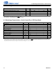
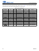
5.1 I/O Pin Characteristics
5.1 I/O Pin Characteristics
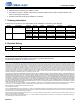
Input and output levels and associated power supply voltage are shown in Table 5-1. Logic levels should not exceed the
corresponding power supply voltage. Typical hysteresis for VL inputs is 250 mV.
. fdf
Table 5-1. I/O Pin Characteristics
Pin Name I/O
Voltage
Reference
Internal
Termination
Driver Receiver
DAO_D1 I/O VL Programmable pull-up CMOS CMOS, with hysteresis
DAI_D2 I/O VL Programmable pull-up CMOS CMOS, with hysteresis
DAO_D2 I/O VL Programmable pull-up CMOS CMOS, with hysteresis
DAI_D1 I/O VL Programmable pull-up CMOS CMOS, with hysteresis
SCLK I/O VL Programmable pull-up CMOS CMOS, with hysteresis
LRCLK I/O VL Programmable pull-up CMOS CMOS, with hysteresis
CLOCK I VL — — CMOS, with hysteresis
MCLK I/O VL Programmable pull-up CMOS CMOS, with hysteresis
MISO/SDA I/O VL Programmable pull-up CMOS/open drain CMOS, with hysteresis
MOSI I/O VL Programmable pull-up CMOS CMOS, with hysteresis
CLK/SCL I/O VL Programmable pull-up CMOS/open drain CMOS, with hysteresis
CS
I/O VL Programmable pull-up CMOS CMOS, with hysteresis
DBCK I/O VL Programmable pull-up CMOS/open drain CMOS, with hysteresis
DBDA I/O VL Programmable pull-up CMOS/open drain CMOS, with hysteresis
RESET
I VL Pull-up — CMOS, with hysteresis
INT
O VL Programmable pull-up CMOS/open drain CMOS, with hysteresis
BUSY
/
I2C_SELECT
I/O VL Programmable pull-up CMOS/open drain CMOS, with hysteresis