
User guide

DS1057F1 22
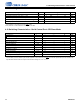
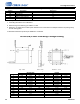
5 Pin Descriptions
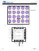
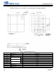
Pin Name CSP
Ball#
QFN
Pin#
Pin Functions
DAO_D1 A1 19 Digital Audio Data Output 1 (Host/Tx/Uplink)
• (O) DAO output 1 for two’s complement serial audio data
DAI_D2 B3 20 Digital Audio Input 2 (Mic In)
• (I) Two’s complement serial audio data input 2 (DAI_D2)
DAO_D2 B4 21 Digital Audio Data Output 2 (Receiver/Speakers)
• (O) Two’s complement serial audio data output 2
DAI_D1 A2 22 Digital Audio Data Input 1 (Host/Rx/Downlink)
• (I) DAI Input 1 for two’s complement serial audio data
SCLK A4 24 Digital Audio Clock
• DAI serial audio bit clock
LRCLK A3 23 Digital Audio Clock
• (I/O) DAI Left/Right Clock (Frame Sync)
CLOCK A5 1 Reference Clock Input
• (I) Reference clock for internal PLL
MCLK B2 18 Master Audio Clock
• (I/O) High-speed serial audio clock (no connect for most applications)
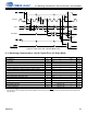
MISO/SDA D3 8 Serial Control Data
• (O) Serial data output for SPI slave mode
• (Open-Drain Bidir) Data for I²C serial control
MOSI D2 9 Serial Control Data
• (I) Serial data input for SPI slave mode
CLK/SCL D4 6 Serial Control Port Clock
• (I) Serial control clock for SPI slave mode
• (Open-Drain Bidir.)Serial control clock for I²C slave
CS
C4 7 Serial Control Port Select
• (I) Chip select for SPI slave mode
DBDA B1 17 Debug Serial Control Data
• (Open-Drain Bidir) Open-drain serial data for the I²C debug serial control port
DBCK C1 13 Debug Serial Control Port Clock
• (Open-Drain Bidir.) Open-drain serial clock for the I²C debug serial control port
RESET
D1 12 Reset
• (I) Active low. Registers are reset to default settings and boot mode selected
INT
C2 11 Interrupt (requires 10 K external pull-up resistor)
• (Open-Drain Output) Active low. Programmable interrupt output
BUSY
/
I2C_SELECT
C3 10 Busy Indicator
• (Open-Drain Output) Active low. DSP busy signal output
• (I) Boot mode select 0 on rising edge of RESET
(selects boot from I
2
C rather than the default SPI)
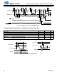
VD B5 4,16 Digital Core and Memory Power
• (I) Power supply for the core and memory section
VPLL — 2 PLL Power
• (I) QFN package only. Power supply for PLL—tie to VD.
VL D5/ 5,14 Digital Interface Power
• (I) Sets voltage reference level for serial audio interfaces and SP
GND C5 3,15 Ground
• (I) Ground reference
Thermal Pad — Thermal Pad (QFN package only)
• (I) Thermal relief pad for optimized heat dissipation. This pad must be connected to GND.