
User guide

15 DS1057F1
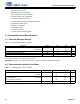
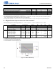
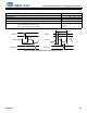
4.5 Thermal Characteristics
4.5 Thermal Characteristics
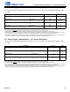
4.6 Digital Interface Specifications and Characteristics
Test Conditions (unless otherwise specified): VL = 1.8 V–3.3 V, VD = 1.0 V–1.2 V; GND = 0 V; T
A
=+25°C.
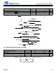
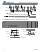
Figure 4-1. Internal Weak Pull-up
Parameter Symbol Min Typ Max Units
QFN junction-to-ambient thermal impedance
1,2
4-layer board
1. To calculate the die temperature for a given power dissipation:
T
j
= Ambient temperature + [ (Power Dissipation in Watts) *
ja
]
2.Four-layer board is specified as a 76 mm X 114 mm, 1.6 mm thick FR-4 material with 1-oz. copper covering 20% of the top and bottom layers and
0.5-oz. copper covering 90% of the internal power plane and ground plane layer
JA
—28 —°C/Watt
WLCSP junction-to-ambient thermal impedance
1,2
4-layer board
JA
—47 —°C/Watt
QFN junction-to-ambient thermal impedance
1,3
2-layer board
3.Two-layer board is specified as a 76 mm X 114 mm, 1.6 mm thick FR-4 material with 1-oz. copper covering 20% of the top and bottom layers.
JA
—85 —°C/Watt
WLCSP junction-to-ambient thermal impedance
1,3
2-layer board
JA
—89 —°C/Watt
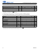
Parameters Test Conditions Symbol Min Typ Max Units
Input leakage current
1
1.Specification is per pin, and does not include current through pull-up.
—— I
in
— — 500 nA
Internal weak pull-up
2
2.The effective pull-up value decreases (more current is provided) with increased VL.
—— — 15—60k
Input capacitance
3
3.This value is by design and not a tested parameter.
—— — —10—pF
VL logic
High-level output voltage
4
4.This value tested with 2-mA drivers enabled on pins.
VL = 3.3 V I
OH
= 2 mA V
OH
VL–0.4 — — V
Low-level output voltage
4
VL = 3.3 V I
OL
= 2 mA V
OL
— — 0.20•VL V
High-level output voltage
4
VL = 1.8 V I
OH
= 1 mA V
OH
VL–0.4 — — V
Low-level output voltage
4
VL = 1.8 V I
OL
= 1 mA V
OL
— — 0.20•VL V
High-level input voltage — — V
IH
0.76•VL — — V
Low-level input voltage — — V
IL
— — 0.30•VL V