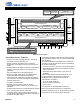
CS48LV12/13 Ultralow Power HD Voice Processors, Featuring SoundClear® Technology • ASR Enhance™ automatic speech recognition (ASR) preprocessing for increased ASR accuracy in noisy Complete easy-to-implement voice solution including all environments essential voice, audio, and speech DSP features for • Voice activity detector (VAD) enables always-on speech flagship smartphones, tablets, and computing products recognition SoundClear Voice™ noise reduction, echo cancellation, • TrulyHandsfree™ voice control b
Voice Activity Detector SoundClear ASR Enhance™ Sensory Inc.
Cirrus Logic Speech Features (CS48LV13 Only) Optional Audio Playback Features Supported (CS48LV13 Only) 1 • ASR Enhance preprocessor for ASR engines • Dolby® postprocessing (enhancement and virtualization) —Improves speech command recognition of ASR • DTS® postprocessing (enhancement and virtualization) engines in noisy environments • Headphone and speaker playback support —Can be applied with VAD described below and optional TrulyHandsfree voice control and/or cloud based ASR Applications Optional Speec
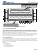
General Description The CS48LV12 and CS48LV13 ultralow power voice processors feature Cirrus Logic’s patented SoundClear® technology to provide a new standard in HD Voice quality performance, functionality, and cost effectiveness. These ICs provide a total voice processing solution for handset and hands-free communications that deliver best-in-class noise reduction, echo cancellation, and speech recognition.
1 Documentation 1 Documentation This document describes the CS48LV12 and CS48LV13 HD voice processors. When evaluating or designing a system around the CS48LV12/13 processors, use this document in conjunction with the documents listed in Table 1-1. Table 1-1.
2.1 Licensing A key feature of both products that enables ease of implementation, quick time to market and performance optimized to a particular ID is the RAPID2 diagnostic and tuning tool. This Microsoft Windows® based tool provides GUI based monitoring and control of all critical SoundClear parameters as well as system level measurements and statistics. RAPID2 tool features are described in Section 3.16. 2.
3.1 Cirrus Logic 32-bit DSP Core Voice Activity Detector SoundClear ASR Enhance™ Sensory Inc.
3.3 Tx Voice DSP Chain The CS48LV13 includes two additional processing groups: 5. Speech DSP Chain 6. Advanced Audio Playback DSP Chain Cirrus Logic provides two specialized tools for controlling and tuning the various processing groups. For voice- and speech-related processing groups, the RAPID2 tool provides real-time analysis and tuning of all parameters. For audio-playback chains, a specialized version of the DSP Composer tool is used for real-time control and tuning.
3.6 Acoustic Echo Cancellation (AEC) adjustments to compensate for changes in device orientation. This results in better off-axis performance than do traditional techniques with fixed acceptance angles. The noise-reduction block uses highly adaptive spatial analysis, spectral analysis, and audio classification to quickly adjust for changes in audio environment and talker position.
3.9 Automatic Level Control (ALC) 3.9 Automatic Level Control (ALC) Tx voice level can vary greatly based on talker loudness, product distance and orientation. By distinguishing between voice and noise levels and adjusting Tx voice level accordingly, the ALC is able to maintain more consistent Tx voice loudness without boosting noise in periods of silence. This improves far-end user experience and product performance when it is held away from the mouth or off-axis. 3.
3.13 Speech DSP Chain 3.13 Speech DSP Chain The CS48LV13 includes Cirrus Logic ASR Enhance preprocessor that removes noise impacting ASR engine performance.
3.15 Power Management The serial control port also includes a pin for flow control of the communications interface (BUSY/I2C_SELECT) and a pin to indicate when the DSP has a message for the host (INT). 3.14.3 PLL-based Clock Generator The low-jitter PLL generates integer or fractional multiples of a reference frequency, which are used to clock the DSP core and peripherals. Through a second PLL divider chain, a dependent clock domain can be output on the DAO port for driving audio converters.
4 Characteristics and Specifications • Multi-mic noise reduction • Single-mic noise reduction • Audio detection and classification • AEC, including path-change detection • Nonlinear residual echo suppression • Tx and Rx automatic level control • Tx and Rx parametric EQ (with graphical interface) • Rx automatic volume control • Speaker out compander • Double-talk detection • Voice activity detection • Tx and Rx comfort noise generation 4 Characteristics and Specifications 4.
4.3 Power Supply Characteristics—1.0 V Power Dissipation 4.3 Power Supply Characteristics—1.0 V Power Dissipation Test Conditions (unless otherwise specified): VD,VPLL=1.0 V, VL=1.8 V, GND = 0 V; all voltages with respect to GND. TA = +25°C. Parameters Core and I/O Operating1 RESET Active3 Hibernate Mode4 Typical Units VD + VPLL2 9.5 mA VL 0.8 mA VD + VPLL2 VL 1.8 mA 1.5 A A A A A VD + VL Sleep Mode5 VPLL2 11 0.147 VD + VPLL2 VL 45 0.147 1.
4.5 Thermal Characteristics 4.5 Thermal Characteristics Symbol Min Typ Max Units QFN junction-to-ambient thermal impedance1,2 Parameter 4-layer board JA — 28 — °C/Watt WLCSP junction-to-ambient thermal impedance1,2 4-layer board JA — 47 — °C/Watt 2-layer board JA — 85 — °C/Watt 2-layer board JA — 89 — °C/Watt QFN junction-to-ambient thermal impedance1,3 WLCSP junction-to-ambient thermal impedance1,3 1.
4.7 Switching Characteristics—RESET 4.7 Switching Characteristics—RESET Parameter RESET minimum pulse width low1 Symbol Min Max Unit Trstl 1 — s All bidirectional pins high-Z after RESET low Trst2z — 100 ns Configuration pins setup before RESET high Trstsu 50 — ns Configuration pins hold after RESET high Trsthld 20 — ns 1.The rising edge of RESET must not occur before the power supplies are stable at their recommended operating values.
4.9 Switching Characteristics—Internal Clock 4.9 Switching Characteristics—Internal Clock Parameter Symbol Min Typ Max Unit Fdclk FCLOCK/256 — 130 MHz Internal DCLK frequency1 (VD, VPLL = 1.2 V) Internal DCLK frequency1 (VD, VPLL = 1.0 V) Fdclk FCLOCK/256 — 80 MHz Internal DCLK period (VD, VPLL = 1.2 V) DCLKP 7.69 — 256/FCLOCK ns Internal DCLK period (VD, VPLL = 1.0 V) DCLKP 12.5 — 256/FCLOCK ns — — 500 — ps Cycle-to-cycle jitter on Internal DCLK or Mastered MCLK2 1.
4.11 Switching Characteristics—Serial Control Port—I2C Slave Mode t spicss CS 0 1 2 tspickl 6 7 0 A0 R/W MSB 5 7 6 tspicsh CLK/SCL fspisck tspickh A6 MOSI A5 LSB tspidsu tspidh t spidov tspicsdz MSB MISO/SDA LSB tspiirqh t spiirql INT t spibsyl BUSY/ I2C_SELECT Figure 4-5. Serial Control Port—SPI Slave Mode Timing 4.
4.12 Switching Characteristics—Digital Audio Slave Input Port tiicckcmd t iicckl 0 1 t iicr 6 tiicf 7 8 t iicckcmd 0 1 6 7 8 CLK/SCL t iicstscl MISO/SDA tiicckh A6 thddo A0 R/W t iicstp f iicck ACK MSB LSB ACK tiicirqh t iicsu t iicbft tiicirql tiich INT t iiccbsyl BUSY/ I2C_SELECT Figure 4-6. Serial Control Port—I2C Slave Mode Timing 4.
4.13 Switching Characteristics—Digital Audio Output Port 4.
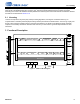
5 Pin Descriptions 5 Pin Descriptions A1 A2 DAO_D1 DAI_D1 A3 A4 A5 LRCLK SCLK CLOCK Top-Down (Through-Package)View 20-Ball WLCSP Package B2 B3 B4 B5 DBDA MCLK DAI_D2 DAO_D2 VD C1 C2 C3 C4 C5 DBCK INT CS GND D1 D2 D4 D5 RESET MOSI CLK/SCL VL BUSY/I2C_SELECT D3 22 DAI_D2 23 DAO_D2 LRCLK 24 DAI_D1 SCLK MISO /SDA 21 20 DAO_D1 B1 19 18 MCLK 17 DBDA 16 VD 15 GND 5 14 VL 6 13 DBCK CLOCK 1 VPLL 2 Thermal Pad GND 3 VD 4 21 9 10 MOSI BUS
5 Pin Descriptions Pin Name CSP Ball# QFN Pin# DAO_D1 A1 19 Digital Audio Data Output 1 (Host/Tx/Uplink) • (O) DAO output 1 for two’s complement serial audio data DAI_D2 B3 20 Digital Audio Input 2 (Mic In) • (I) Two’s complement serial audio data input 2 (DAI_D2) DAO_D2 B4 21 Digital Audio Data Output 2 (Receiver/Speakers) • (O) Two’s complement serial audio data output 2 DAI_D1 A2 22 Digital Audio Data Input 1 (Host/Rx/Downlink) • (I) DAI Input 1 for two’s complement serial audio data
5.1 I/O Pin Characteristics 5.1 I/O Pin Characteristics Input and output levels and associated power supply voltage are shown in Table 5-1. Logic levels should not exceed the corresponding power supply voltage. Typical hysteresis for VL inputs is 250 mV. . fdf Table 5-1.
6 Package Dimensions 6 Package Dimensions 20-BALL WLCSP (2.25 mm x 2.0 mm Body) Package Drawing A B C D 1 2 3 4 5 Table 6-1. WLCSP Package Dimension Symbol A S A1 E D SE SD E1 D1 e b n 24 Description Total thickness Wafer thickness Standoff Body size Ball/bump pitch Edge ball center-to-center Pitch Ball diameter Ball/bump width Ball/bump count X Y X Y X Y Dimensions 0.495 ±0.04 0.305 ±0.025 0.190 ±0.015 2 2.25 0.2 BSC1 — BSC 1.2 BSC 1.6 BSC 0.4 BSC 0.25 0.216–0.
6 Package Dimensions Table 6-1. WLCSP Package Dimension (Cont.) Symbol aaa bbb ccc ddd eee Description Package edge tolerance Wafer flatness Coplanarity Ball/bump offset (package) Ball/bump offset (ball) Dimensions 0.05 0.1 0.03 0.15 0.05 1.Basic spacing between centers. 7. Controlling dimensions are in millimeters. 8. Dimensioning and tolerancing per ASME Y 14.5M. 9. Dimension “b” applies to the solder sphere diameter and is measured at the midpoint between the package body and the seating plane. 10.
7 Ordering Information 1. Controlling dimensions are in millimeters. 2. Dimensioning and tolerancing per ASME Y 14.5M. 3. This drawing conforms to JEDEC outline MS-012, variation VGGD-6 with exception of features D2, E2, and L, which are per supplier designation. 4. Recommended reflow profile is per JEDEC/IPC J-STD-020. 7 Ordering Information Check with your local Cirrus Logic representative for the availability of Automotive grade packages.