
Manual


Table Of Contents
- 1 Documentation Strategy
- 2 Overview
- 3 Code Overlays
- 4 Hardware Functional Description
- 5 Characteristics and Specifications
- 5.1 Absolute Maximum Ratings
- 5.2 Recommended Operations Conditions
- 5.3 Digital DC Characteristics
- 5.4 Power Supply Characteristics
- 5.5 Thermal Data (48-pin LQFP)
- 5.6 Switching Characteristics-RESET
- 5.7 Switching Characteristics-XTI
- 5.8 Switching Characteristics-Internal Clock
- 5.9 Switching Characteristics-Serial Control Port-SPI Slave Mode
- 5.10 Switching Characteristics-Serial Control Port-SPI Master Mode
- 5.11 Switching Characteristics-Serial Control Port-I2C Slave Mode
- 5.12 Switching Characteristics-Serial Control Port-I2C Master Mode
- 5.13 Switching Characteristics-Digital Audio Slave Input Port
- 5.14 Switching Characteristics-DSD Slave Input Port
- 5.15 Switching Characteristics-Digital Audio Output (DAO) Port
- 6 Ordering Information
- 7 Environmental, Manufacturing, and Handling Information
- 8 Device Pinout Diagrams
- 9 Package Mechanical Drawings
- 10 Revision History
9 DS734F5
4.4 Application Code Security
4.3.3 Pads
The CS485xx I/Os operate from the 3.3 V supply and are 5 V tolerant.
4.4 Application Code Security
The external program code may be encrypted by the programmer to protect any intellectual property it may contain. A
secret, customer-specific key is used to encrypt the program code that is to be stored external to the device. Contact your
local Cirrus representative for details.
5 Characteristics and Specifications
Note: All data sheet minimum and maximum timing parameters are guaranteed over the rated voltage and temperature.
All data sheet typical parameters are measured under the following conditions: T = 25° C, C
L
= 20 pF,
VDD = VDDA = 1.8 V, VDDIO = 3.3 V, GNDD = GNDIO = GNDA = 0 V.
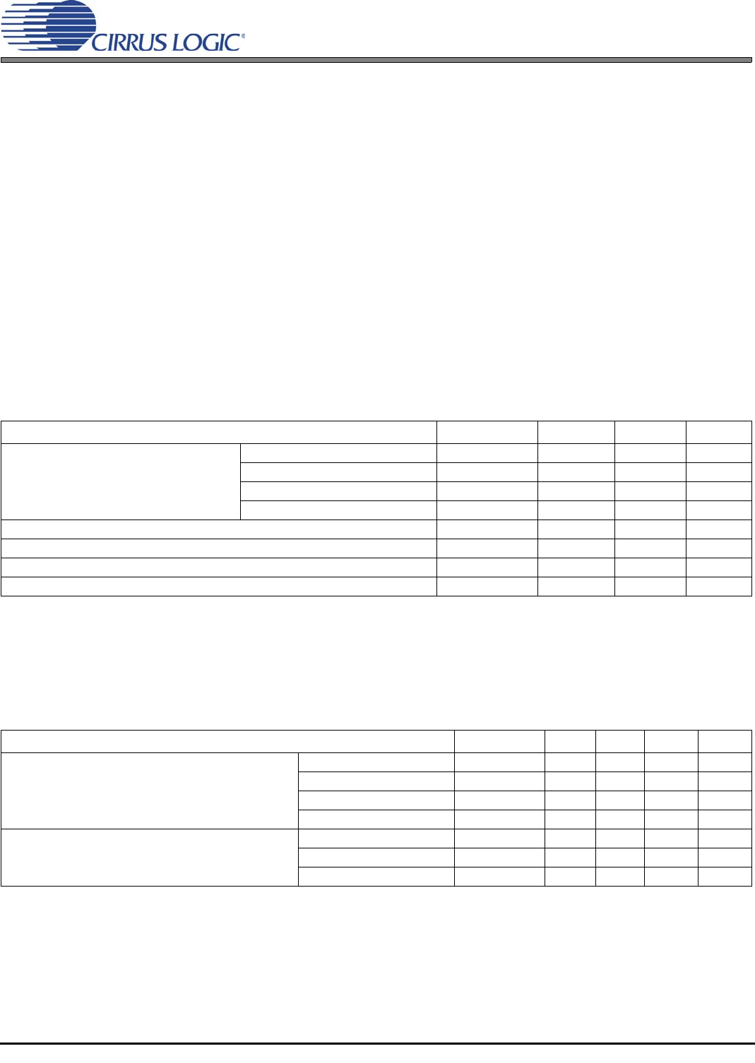
5.1 Absolute Maximum Ratings
(GNDD = GNDIO = GNDA = 0 V; all voltages with respect to 0 V)
WARNING: Operation at or beyond these limits may result in permanent damage to the device. Normal operation is not
guaranteed at these extremes.
5.2 Recommended Operations Conditions
(GNDD = GNDIO = GNDA = 0 V; all voltages with respect to 0 V)
Note: It is recommended that the 3.3 V IO supply come up ahead of or simultaneously with the 1.8 V core supply.
5.3 Digital DC Characteristics
(Measurements performed under static conditions.)
Parameter Symbol Min Max Unit
DC power supplies: Core supply VDD –0.3 2.0 V
PLL supply VDDA –0.3 3.6 V
I/O supply VDDIO –0.3 3.6 V
|VDDA–VDDIO| — — 0.3 V
Input pin current, any pin except supplies I
in
—±10mA
Input voltage on PLL_REF_RES V
filt
–0.3 3.6 V
Input voltage on I/O pins V
inio
–0.3 5.0 V
Storage temperature T
stg
–65 150 °C
Parameter Symbol Min Typ Max Unit
DC power supplies: Core supply VDD 1.71 1.8 1.89 V
PLL supply VDDA 3.13 3.3 3.46 V
I/O supply VDDIO 3.13 3.3 3.46 V
|VDDA–VDDIO| — — 0 — V
Ambient operating temperature T
A
——— °C
–CQZ — 0 — +70 —
–DQZ — –40 — +85 —