
Manual


Table Of Contents
- 1 Documentation Strategy
- 2 Overview
- 3 Code Overlays
- 4 Hardware Functional Description
- 5 Characteristics and Specifications
- 5.1 Absolute Maximum Ratings
- 5.2 Recommended Operations Conditions
- 5.3 Digital DC Characteristics
- 5.4 Power Supply Characteristics
- 5.5 Thermal Data (48-pin LQFP)
- 5.6 Switching Characteristics-RESET
- 5.7 Switching Characteristics-XTI
- 5.8 Switching Characteristics-Internal Clock
- 5.9 Switching Characteristics-Serial Control Port-SPI Slave Mode
- 5.10 Switching Characteristics-Serial Control Port-SPI Master Mode
- 5.11 Switching Characteristics-Serial Control Port-I2C Slave Mode
- 5.12 Switching Characteristics-Serial Control Port-I2C Master Mode
- 5.13 Switching Characteristics-Digital Audio Slave Input Port
- 5.14 Switching Characteristics-DSD Slave Input Port
- 5.15 Switching Characteristics-Digital Audio Output (DAO) Port
- 6 Ordering Information
- 7 Environmental, Manufacturing, and Handling Information
- 8 Device Pinout Diagrams
- 9 Package Mechanical Drawings
- 10 Revision History
22 DS734F5
9 Package Mechanical Drawings
9 Package Mechanical Drawings
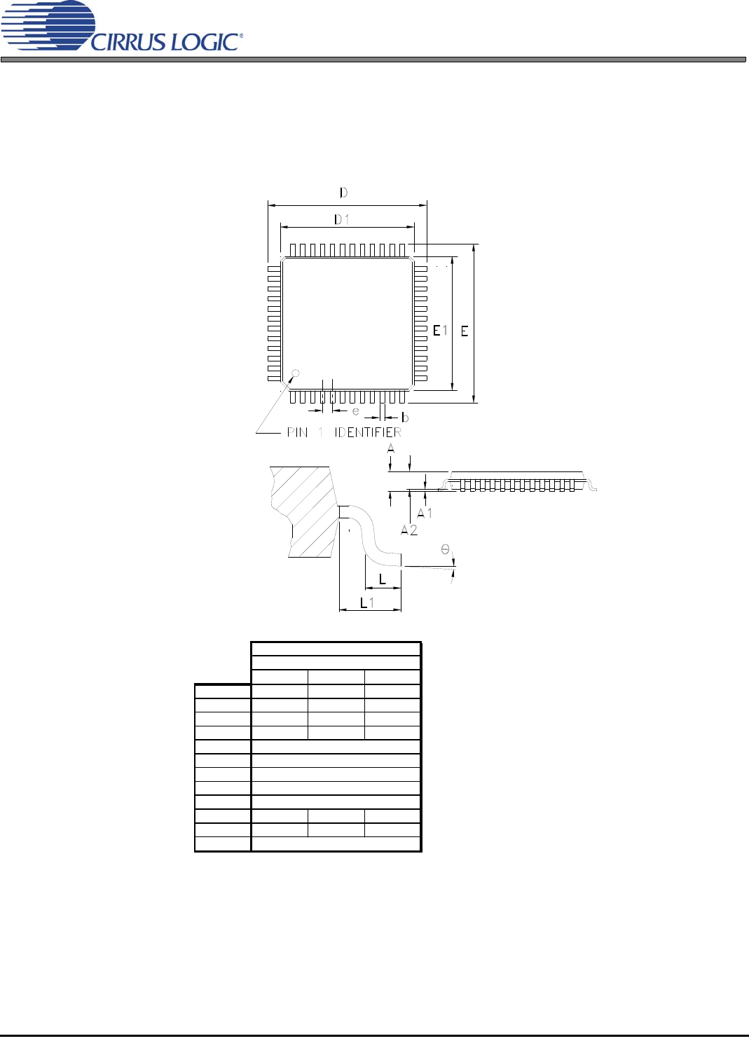
9.1 48-pin LQFP Package Drawing
Figure 9-1. 48-pin LQFP Package Drawing
48 LD LQFP (7 x 7 x 1.4 mm body)
Number of Leads
48
MIN NOM MAX
A1.60
A1 0.05 0.15
A2 1.35 1.40 1.45
b 0.17 0.22 0.27
D9.00BSC
D1 7.00 BSC
e0.50BSC
E9.00BSC
E1 7.00 BSC
theta 0 7
L 0.45 0.60 0.75
L1 1.00 REF
NOTES:
1) Reference document: JEDEC MS-026
2) All dimensions are in millimeters and controlling dimension is in millimeters.
3) D1 and E1 do not include mold flash which is 0.25 mm max. per side.A1
4) Dimension b does not include a total allowable dambar protrusion of 0.08 mm max.