CS44800 8-Channel Digital Amplifier Controller Features > 100 dB Dynamic Range - System Level Eliminates AM Frequency Interference < 0.03% THD+N @ 1 W - System Level Programmable Load Compensation Filters 32 kHz to 192 kHz Sample Rates Support for up to 40 kHz Audio Bandwidth Internal Oscillator Circuit Supports 24.576 MHz Digital Volume Control with Soft Ramp to 54 MHz Crystals – Integrated Sample Rate Converter (SRC) – – +24 to -127 dB in 0.
CS44800 General Description The CS44800 is a multi-channel digital-to-PWM Class D audio system controller including interpolation, sample rate conversion, half- and full-bridge PWM driver outputs, and power supply rejection feedback in a 64-pin LQFP package.The architecture uses a direct-to-digital approach that maintains digital signal integrity to the final output filter, minimizing analog interference effects which negatively affect system performance.
CS44800 TABLE OF CONTENTS 1. CHARACTERISTICS AND SPECIFICATIONS ...................................................................................... 8 SPECIFIED OPERATING CONDITIONS .............................................................................................. 8 ABSOLUTE MAXIMUM RATINGS ........................................................................................................ 8 DC ELECTRICAL CHARACTERISTICS .....................................................................
CS44800 7.1.1 Increment (INCR) ................................................................................................................. 50 7.1.2 Memory Address Pointer (MAPx) ......................................................................................... 50 7.2 CS44800 I.D. and Revision Register (address 01h) (Read Only) ................................................. 50 7.2.1 Chip I.D. (Chip_IDx) ..........................................................................................
CS44800 7.19.1 Channel Compensation Filter - Fine Adjust (CHXX_FINE[5:0]) ......................................... 63 7.20 Interrupt Mode Control (address 28h) ......................................................................................... 63 7.20.1 Interrupt Pin Control (INT1/INT0) ....................................................................................... 63 7.20.2 Overflow Level/Edge Select (OVFL_L/E) ........................................................................... 64 7.
CS44800 LIST OF FIGURES Figure 1.Performance Characteristics Evaluation Active Filter Circuit ...................................................... 10 Figure 2.XTI Timings ................................................................................................................................. 11 Figure 3.SYS_CLK Timings ...................................................................................................................... 12 Figure 4.PWMOUTxx Timings .................................
CS44800 LIST OF TABLES Table 1. Common DAI_MCLK Frequencies .............................................................................................. 25 Table 2. DAI Serial Audio Port Channel Allocations ................................................................................. 27 Table 3. Load Compensation Example Settings ....................................................................................... 32 Table 4. Typical PWM Switch Rate Settings .........................................
CS44800 1. CHARACTERISTICS AND SPECIFICATIONS (All Min/Max characteristics and specifications are guaranteed over the Specified Operating Conditions. Typical performance characteristics and specifications are derived from measurements taken at nominal supply voltages and TA = 25°C.) SPECIFIED OPERATING CONDITIONS (GND = 0 V, all voltages with respect to ground) Parameter Symbol Min Typ Max Units DC Power Supply Digital 2.5 V VD 2.37 2.5 2.63 V XTAL (Note 1) 2.5 V 3.3 V 5.0 V VDX 2.37 3.
CS44800 DC ELECTRICAL CHARACTERISTICS (GND = 0 V, all voltages with respect to ground; DAI_MCLK = 12.288 MHz, XTAL = 24.576 MHz, PWM Switch Rate = 384 kHz unless otherwise specified.) Parameter Symbol Min Typ Max Units ID IDX IDP ILS ILC - 150 2 1.2 150 250 - mA mA mA µA µA - 387 500 mW - 15 40 - dB dB - 80 - µA Normal Operation (Note 4) Power Supply Current (Note 5) Power Dissipation VD = 2.5 V VDX = 3.3 V VDP = 3.3 V VLS = 3.3 V VLC = 3.3 V (Note 6) VD=2.
CS44800 PWM OUTPUT PERFORMANCE CHARACTERISTICS (Logic “0” = GND = 0 V; Logic “1” = VLS = VLC; VD = 2.5 V; DAI_MCLK = 12.288 MHz; XTAL= 24.576 MHz; PWM Switch Rate = 384 kHz; Fs = 32 kHz to 192 kHz; Measurement bandwidth is 10 Hz to 20 kHz unless otherwise specified; Performance measurements taken with a full-scale 997 Hz.
CS44800 PWM FILTER CHARACTERISTICS (Logic “0” = GND = 0 V; Logic “1” = VLS = VLC; VD = 2.5 V; DAI_MCLK = 12.288 MHz; XTAL = 24.576 MHz; PWM Switch Rate = 384 kHz; Fs = 32 kHz to 192 kHz; Measurement bandwidth is 10 Hz to 20 kHz unless otherwise specified.) Parameter Digital Filter Response (Note 12) Passband OSRATE = 0b OSRATE = 1b (Note 13) OSRATE = 0b OSRATE = 1b (Note 13) Group Delay De-emphasis Error (Relative to 1 kHz) to -0.01 dB corner to -3 dB corner to -0.
CS44800 SWITCHING CHARACTERISTICS - SYS_CLK (VD = 2.5 V, VDP = VLC = VDX = 3.3 V, VLS = 2.5 V to 5.0 V, Cload = 50 pF) Parameter SYS_CLK Period Symbol Min tsclki 18.518 45 SYS_CLK Duty Cycle Typ Max Unit --- --- ns 50 55 % SYS_CLK tsclki Figure 3. SYS_CLK Timings SWITCHING CHARACTERISTICS - PWMOUTA1-B4 (VD = 2.5 V, VLS = VLC = VDX = 3.3 V, VDP = 3.3 V to 5.0 V unless otherwise specified, Cload = 10 pF) Parameter PWMOUTxx Period Symbol Min Typ Max Unit tpwm 2.60 - 1.
CS44800 SWITCHING CHARACTERISTICS - DAI INTERFACE (VD = 2.5 V, VDX = VDP = VLC = 3.3 V, VLS = 2.5 V to 5.0 V; Inputs: Logic 0 = GND, Logic 1 = VLS.
CS44800 SWITCHING CHARACTERISTICS - CONTROL PORT - I²C FORMAT (VD = 2.5 V, VDX = VDP = VLS = 3.3 V; VLC = 2.5 V to 5.0 V; Inputs: Logic 0 = GND, Logic 1 = VLC, CL = 30 pF) Parameter Symbol Min Max Unit SCL Clock Frequency fscl - 100 kHz Bus Free Time between Transmissions tbuf 4.7 - µs Start Condition Hold Time (prior to first clock pulse) thdst 4.0 - µs Clock Low time tlow 4.7 - µs Clock High Time thigh 4.0 - µs Setup Time for Repeated Start Condition tsust 4.
CS44800 SWITCHING CHARACTERISTICS - CONTROL PORT - SPI FORMAT (VD = 2.5 V, VDP = VLS = 3.3 V; VLC = 2.5 V to 5.0 V; Inputs: Logic 0 = GND, Logic 1 = VLC, CL = 30 pF) Parameter Symbol Min Typ Max Units CCLK Clock Frequency fsck 0 - 6.0 MHz CS High Time between Transmissions tcsh 1.
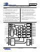
CS44800 PSR_MCLK PSR_DATAL PSR_SYNC PSR_RESET GND PWMOUTB2- PWMOUTB2+ VDP PWMOUTA2- PWMOUTA2+ GND PWMOUTB1- PWMOUTB1+ VDP PWMOUTA1- PWMOUTA1+ 2.
CS44800 PS_SYNC 3 Power Supply Synchronization Clock (Output) - The PWM synchronized clock to the switch mode power supply. XTI 5 Crystal Oscillator Input (Input) - Crystal Oscillator input or accepts an external clock input signal that is used to drive the internal PWM core logic. XTO 6 Crystal Oscillator Output (Output) - Crystal Oscillator output. SYS_CLK 8 External System Clock (Output) - Clock output. This pin provides a divided down clock derived from the XTI input.
CS44800 GPIO2 33 General Purpose Input, Output (Input/Output) - This pin is configured as an input following a RST condition. It can be configured as a general purpose input or output which can be individually controlled by the Host Controller. GPIO1 34 General Purpose Input, Output (Input/Output) - This pin is configured as an input following a RST condition. It can be configured as a general purpose input or output which can be individually controlled by the Host Controller.
CS44800 GND DS632F1 1, 4, 18, 28, 36, 42, Digital Ground (Input) - Ground reference for digital circuits.
CS44800 2.1 I/O Pin Characteristics Signal Name Power Rail I/O Driver Receiver RST VLC Input - 2.5 V and 3.3/5.0 V TTL Compatible. SCL/CCLK VLC Input - 2.5 V and 3.3/5.0 V TTL Compatible, with Hysteresis. SDA/CDOUT VLC Input / Output 2.5-5.0 V, 2.5 V and 3.3/5.0 V TTL Compatible, with Hysteresis. CMOS/Open Drain AD0/CS VLC Input - 2.5 V and 3.3/5.0 V TTL Compatible, Internal pull-up. AD1/CDIN VLC Input - 2.5 V and 3.3/5.0 V TTL Compatible, Internal pull-up.
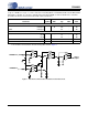
CS44800 0.1 µF 0.01 µF 0.1 µF 0.01 µF 0.1 µF 0.01 µF 0.1 µF 0.01 µF 3. TYPICAL CONNECTION DIAGRAMS +3.3 V to +5.0 V 10 µF +2.5 V + 10 µF 0.1 µF 0.01 µF VDP PWMOUTA1+ PWMOUTA1GPIO1 VD PWMOUTB1+ PWMOUTB1- VD 0.1 µF 0.01 µF 0.01 µF 0.1 µF 24.576 MHz XTAL to 54 MHz +2.5 V to +5.
0.1 µF 0.01 µF 0.1 µF 0.1 µF 0.01 µF 0.01 µF 0.1 µF 0.01 µF CS44800 +3.3 V to +5.0 V 10 µF +2.5 V + 10 µF 0.1 µF 0.01 µF VDP PWMOUTA1+ PWMOUTA1- VD PWMOUTB1+ PWMOUTB1- VD 0.1 µF 0.01 µF CS44800 +3.3 V to +5.0 V VDX 0.01 µF 0.1 µF 24.576 MHz XTAL to 54 MHz GPIO2 PWM IN1 OUT1 PWM IN2 OUT2 Front Left CONTROL STATUS PWMOUTA2+ PWMOUTA2- PWM IN1 OUT1 PWMOUTB2+ PWMOUTB2- PWM IN2 OUT2 Front Right Surr.
CS44800 4. APPLICATIONS 4.1 Overview The CS44800 is a multi-channel digital-to-PWM Class D audio system controller including interpolation, sample rate conversion, half- and full-bridge PWM driver outputs, and power supply rejection feedback in a 64-pin LQFP package. The architecture uses a direct-to-digital approach that maintains digital signal integrity to the final output filter, minimizing analog interference effects which negatively affect system performance.
CS44800 • Digital volume control with soft ramp. • Individual channel volume gain, attenuation and mute capability; +24 to -127 dB in 0.25 dB steps. • Master volume attenuation; +24 to -127 dB in 0.25 dB steps. • Peak Detect and Volume Limiter with programmable attack and release rates. • Signal-clipping interrupt indicator. Additional Features • Contains a two-stage digital output filter for speaker impedance compensation.
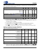
CS44800 4.3.1 FsIn Domain Clocking Common DAI_MCLK frequencies and sample rates are shown in Table 1. Mode (sample-rate range) Sample Rate (kHz) DAI_MCLK/LRCK Ratio −> 32 Single Speed (4 to 50 kHz) 44.1 48 DAI_MCLK/LRCK Ratio −> 64 Double Speed (50 to 100 kHz) 88.2 96 DAI_MCLK/LRCK Ratio −> 176.4 Quad Speed (100 to 200 kHz) 192 DAI_MCLK (MHz) 256x 8.1920 11.2896 12.2880 128x 8.1920 11.2896 12.2880 64x n/a n/a 384x 12.2880 16.9344 18.4320 192x 12.2880 16.9344 18.4320 96x n/a n/a 512x 16.3840 22.
CS44800 XTI Y1 C1 XTO L1 C3 C2 Figure 15. 3rd Overtone Crystal Configuration Appropriate clock dividers for each functional block and a programmable divider to support an output for switched-mode power supply synchronization are provided. The clock generation for the CS44800 is shown in the Figure 16. XTO PWM Master Clock Divider XTI PWM_MCLK System Clock Divider PWM Modulator Clock Divider SYS_CLK MOD_MCLK Power Supply Sync.
CS44800 4.4 FsIn Clock Domain Modules 4.4.1 Digital Audio Input Port The CS44800 interfaces to an external Digital Audio Processor via the Digital Audio Input serial port, the DAI serial port. The DAI port has 4 stereo data inputs with support for I²S, left-justified and right-justified formats. The DAI port operates in slave operation only, where DAI_LRCK, DAI_SCLK and DAI_MCLK are always inputs.
CS44800 4.4.1.1 I²S Data Format For I²S, data is received most significant bit first, one DAI_SCLK delay after the transition of DAI_LRCK, and is valid on the rising edge of DAI_SCLK. For the I²S format, the left channel data is presented when DAI_LRCK is low; the right channel data is presented when DAI_LRCK is high.
CS44800 4.4.1.3 Right-Justified Data Format In the right-justified format, data is received most significant bit first and with the least significant bit presented on the last DAI_SCLK before the DAI_LRCK transition and is valid on the rising edge of DAI_SCLK. For the right-justified format, the left channel data is presented when DAI_LRCK is high and the right channel data is presented when DAI_LRCK is low. Either 16 bits per sample or 24 bits per sample are supported.
CS44800 4.4.1.5 One Line Mode #2 In One Line mode #2 format, data is received most significant bit first on the first DAI_SCLK after a DAI_LRCK transition and is valid on the rising edge of DAI_SCLK. DAI_SCLK must operate at a 256 Fs rate. DAI_LRCK identifies the start of a new frame and is equal to the sample period. DAI_LRCK is sampled as valid on the same clock edge as the most significant bit of the first data sample and must be held high for 128 DAI_SCLK periods.
CS44800 4.4.2 Auto Rate Detect The CS44800 will automatically determine the incoming sample rate, DAI_LRCK, to master clock, DAI_MCLK, ratio and configure the appropriate internal clock divider such that the sample rate convertor receives the required clock rate. A minimum DAI_MCLK rate of 128Fs is required for proper operation. The supported DAI_MCLK to DAI_LRCK ratios are shown in Table 1 on page 26. 4.4.3 De-Emphasis The CS44800 includes on-chip digital de-emphasis filters.
CS44800 4.5 4.5.1 FsOut Clock Domain Modules Sample Rate Converter One of the characteristics of a PWM amplifier is that the frequency content of out-of-band noise generated by the modulator is dependent on the PWM switching frequency. The power stage external LC and snubber filter component values are based on this switching frequency.
CS44800 ger (addresses 09h - 10h)” on page 58. Volume control changes are programmable to ramp in increments of 0.125 dB at a variable rate controlled by the SZC[1:0] bits. Each PWM channel output can be independently muted via mute control bits in the register “Channel Mute (address 13h)” on page 60. When enabled, each CHXX_MUTE bit attenuates the corresponding PWM channel to its maximum value (-127 dB).
CS44800 Fsin (kHz) Fsout (kHz) Quant Level using SRC 32, 44.1, 48, 88.2, 96, 176.4, 192 32, 44.1, 48, 88.2, 96, 176.4, 192 384 421.875 64 64 64 64 OSRATE 1 2 1 2 PWM Required XTAL Switch Rate or SYS_CLK (kHz) (MHz) 384 24.576 768 49.152 421.875 27.000 843.75 54.000 Table 4. Typical PWM Switch Rate Settings 4.5.6 Interpolation Filter The times 2 (2x) interpolation filter is part of the Quantizer and is used to up sample the data to support a higher PWM switch rate.
CS44800 4.5.10 Power Supply Rejection (PSR) Real-Time Feedback Inherent to most Class D power amplifier solutions is the requirement for a clean and well-regulated high voltage power supply. Any noise or tones present on the power rail will couple through each channel’s power MOSFET output device. These spurious distortion components on the output signal consist of discrete tones, which can be audible from the speaker, and tones that modulate around the audio signal being played.
CS44800 4.6 Control Port Description and Timing The control port is used to access the registers, allowing the CS44800 to be configured for the desired operational modes and formats. The operation of the control port may be completely asynchronous with respect to the audio sample rates. However, to avoid potential interference problems, the control port pins should remain static if no operation is required. The control port has 2 modes: SPI and I²C, with the CS44800 acting as a slave device.
CS44800 4.6.2 I²C Mode In I²C mode, SDA is a bidirectional data line. Data is clocked into and out of the part by the clock, SCL. There is no CS pin. Pins AD0 and AD1 form the two least significant bits of the chip address and should be connected through a resistor to VLC or GND as desired. The state of the pins is sensed while the CS44800 is being reset. The signal timings for a read and write cycle are shown in Figure 25 and Figure 26.
CS44800 Receive acknowledge bit. Receive byte, contents of selected register. Send acknowledge bit. Send stop condition. Each byte is separated by an acknowledge bit. 4.6.3 GPIOs The CS44800 GPIO pins will have the following features: 4.6.4 • Data direction control. • Programmable open-drain or push-pull driver when configured as an output pin. • Maskable interrupt for GPIO[3:0] pins when set as a general purpose input. • Level-sensitive or edge-trigger event selector for all GPIO pins.
CS44800 5. POWER SUPPLY, GROUNDING, AND PCB LAYOUT The CS44800 requires a 2.5 V digital power supply for the core logic. In order to support a number of PWM backend solutions, separate VDP power pins are provided to condition the interface signals to support up to 5.0 V levels. The VDP power pins control the voltage levels for all PWM interface signals, PSR interface signals and GPIO for control and status.
CS44800 Figure 28 shows the recommended crystal circuit layout. U1 is the CS44800. C1 and C2 are the VDX power supply decoupling capacitors. Y1 is the crystal and C3, C4, L1 and C5 are the associated components for the crystal circuit. L1 and C5 are only used for 3rd overtone crystals. C3 and C4 should have a C0G (NPO) dielectric. Care should be taken to minimize the distance between the CS44800 XTI/XTO pins and C3.
CS44800 Figure 29 shows the recommended PSR circuit layout. See the CS4461 datasheet for further details on the input buffer and other associated external components. U1 is the CS4461 and U2 is the input buffer op-amp. All supply decoupling should be placed as close as possible to their respective power supply pins. C4 should have a C0G (NPO) dielectric and be placed as close as possible to the CS4461 AIN+/- pins.
CS44800 5.1 Reset and Power-Up Reliable power-up can be accomplished by keeping the device in reset until the power supplies, clocks, and configuration pins are stable. It is also recommended that the RST pin be activated if the voltage supplies drop below the recommended operating condition to prevent power-glitch- related issues. When RST is low, the CS44800 enters a low-power mode and all internal states are reset, including the control port and registers.
CS44800 6. When driving a single-ended (half-bridged) power output stage, set the RAMP[1:0] bits to ‘11’b and the required ramp speed, to initiate a ramp cycle when the channel is powered on. Set MIN_PULSE[4:0] to ‘00000’b. 7. Set the PDN bit to ‘0’b to take the CS44800 out of the power-down state. 8. Start all clocks on the DAI interface (DAI_MCLK, DAI_SCLK, DAI_LRCK). This will initiate the SRC to begin the lock sequence.
Set PSR_RESET = 1b Set PSR_EN = 1b Set PSR_EN = 0b Read DEC_OUTD[23:0] Y 3FEF90h < DEC_OUTD[23:0] < 400FFFh? N Done Y DEC_OUTD[23:0] > 400FFFh? N CPSR =CPSR - 9Bh CPSR =CPSR + 9Bh Figure 30. PSR Calibration Sequence 5.1.4 Recommended Power-Down Sequence 1. Mute all channel outputs by setting the corresponding CHxx_MUTE bits to ‘1’b. 2.
DS632F1 8. Set the PDN bit to ‘1’b to put the CS44800 in the power down state.
6. REGISTER QUICK REFERENCE Addr 01h Function ID / Rev. page 50 default 02h Clock Config / Power Control 03h Chnl Power Down 04h Misc. Config. 05h Ramp Config 06h Vol Control Config page 51. page 52. page 53 page 54 page 55 07h Master Vol. - Integer page 57 08h default default default default default DS632F1 default Channel B4 Vol. Control - Integer page 59.
DS632F1 Addr Function 7 6 5 4 3 2 1 0 11h Channel Vol. Control 1-Fraction CHB2_FVOL1 CHB2_FVOL0 CHA2_FVOL1 CHA2_FVOL0 CHB1_FVOL1 CHB1_FVOL0 CHA1_FVOL1 CHA1_FVOL0 page 59. default 12h Channel Vol. Control 2-Fraction 13h Channel Mute 14h Channel Invert page 59 page 60 page 60 default default default 15h Peak Limiter Control 16h Limiter Attack Rate 17h Limiter Release Rate page 61 page 61 page 62 18h default default Chnl B2 Comp.
Addr 21h Function Chnl A3 Comp. Filter - Fine Adj page 63 22h default Chnl B3 Comp. Filter - Coarse Adj page 62 23h default Chnl B3 Comp. Filter - Fine Adj page 63 24h default Chnl A4 Comp. Filter - Coarse Adj page 62 25h default Chnl A4 Comp. Filter - Fine Adj page 63 26h default Chnl B4 Comp. Filter - Coarse Adj page 62 27h default Chnl B4 Comp.
DS632F1 Addr 31h Function PWM Config page 68 default 32h PWM Minimum Pulse Width 33h PWMOUT Delay page 69 page 70 34h default PSR_Decimator Scaled page 74 36h default PSR / Power Supply Config page 73 35h default default PSR_Decimator Scaled page 74 default 37h PSR_Decimator Scaled 38h Reserved 39h Reserved 3Ah Reserved 3Bh PSR_Decimator Outd 3Ch PSR_Decimator Outd 3Dh PSR_Decimator Outd page 74 default default default default page 75 page 75 page 75 default defaul
CS44800 7. REGISTER DESCRIPTION All registers are read/write except for I.D. and Revision Register, Interrupt Status and Decimator OutD registers which are read only. See the following bit definition tables for bit assignment information. The default state of each bit after a power-up sequence or reset is listed in each bit description. 7.1 Memory Address Pointer (MAP) Not a register 7 INCR 7.1.
CS44800 7.3 Clock Configuration and Power Control (address 02h) 7 6 5 EN_SYS_CLK SYS_CLK_DIV1 SYS_CLK_DIV0 7.3.1 4 PWM_MCLK_DIV1 3 2 1 0 PWM_MCLK_DIV0 PDN_XTAL PDN_OUTPUT_MODE PDN Enable SYS_CLK Output (EN_SYS_CLK) Default = 1 Function: This bit enables the driver for the SYS_CLK signal. If the SYS_CLK output is unused, this bit should be set to ‘0’b to disable the driver. 7.3.
CS44800 7.3.5 Power Down Output Mode (PDN_OUTPUT_MODE) Default = 0 0 - PWM Outputs are driven low during power down 1 - PWM Outputs are driven to the inactive state during power down Function: This bit is used to select the power-down state of the PWM output signals. When set to 0, each channel which has been powered down, following the ramp-down cycle if enabled, will drive the output signals, PWMOUTxx+ and PWMOUTxx-, low.
CS44800 7.5 Misc. Configuration (address 04h) 7 DIF2 7.5.1 6 DIF1 5 DIF0 4 RESERVED 3 AM_FREQ_HOP 2 FREEZE 1 DEM1 0 DEM0 Digital Interface Format (DIFX) Default = 001 Function: These bits select the digital interface format used for the DAI Serial Port. The required relationship between the Left/Right clock, serial clock, and serial data is defined by the Digital Interface Format and the options are detailed in Figures 17 - 22.
CS44800 7.5.4 De-Emphasis Control (DEM[1:0]) Default = 00 00 - no de-emphasis 01 - 32 kHz de-emphasis filter 10 - 44.1 kHz de-emphasis filter 11 - 48 kHz de-emphasis filter Function: Enables the appropriate digital filter to maintain the standard 15 ms/50 ms digital de-emphasis filter response. 7.6 Ramp Configuration (address 05h) 7 RESERVED 7.6.
CS44800 7.7 Volume Control Configuration (address 06h) 7 SNGVOL 7.7.1 6 SZC1 5 SZC0 4 RESERVED 3 MUTE_50/50 2 SRD_ERR 1 SRU_ERR 0 AMUTE Single Volume Control (SNGVOL) Default = 0 Function: The individual channel volume levels are independently controlled by their respective Volume Control registers when this function is disabled. When enabled, the volume on all channels is determined by the A1 Channel Volume Control register. The other Volume Control registers are ignored. 7.7.
CS44800 trol changes, by the Soft and Zero Cross bits (SZC[1:0]). This bit does not cause a mute condition to occur. The MUTE_50/50 bit only defines operation during a normal mute condition. When MUTE_50/50 is set and a mute condition occurs, PSR will not affect the output of the modulator, regardless if PSR is enabled. Output noise may be increased in this case if the noise on the high voltage power supply is greater than the system noise.
CS44800 7.8 Master Volume Control - Integer (address 07h) 7 MSTR_IVOL7 7.8.1 6 MSTR_IVOL6 5 MSTR_IVOL5 4 MSTR_IVOL4 3 MSTR_IVOL3 2 MSTR_IVOL2 1 MSTR_IVOL1 0 MSTR_IVOL0 Master Volume Control - Integer (MSTR_IVOL[7:0]) Default = 00000000 Function: The Master Volume Control - Integer register allows global control of the signal levels on all channels in 1 dB increments from +24 to -127 dB. Volume settings are decoded as shown in Table 6.
CS44800 1. Convert the decimal integer to binary. This is MSTR_IVOL[7:0]. 2. Select the bit representation of the desired 0.25 fractional increment. This is MSTR_FVOL[1:0]. 3. Concatenate MSTR_IVOL[7:0]: MSTR_FVOL[1:0] to form a 10-bit binary value. 4. Perform a 2’s complement conversion on all 10 bits. The upper 8 bits are now the new MSTR_FVOL[7:0] and the two lower bits are MSTR_FVOL[1:0]. To convert from a 2’s complement integer:fraction value to a negative decimal, do the following: 1.
CS44800 7.10 Channel XX Volume Control - Integer (addresses 09h - 10h) 7 CHXX_IVOL7 6 CHXX_IVOL6 5 CHXX_IVOL5 4 CHXX_IVOL4 3 CHXX_IVOL3 2 CHXX_IVOL2 1 CHXX_IVOL1 0 CHXX_IVOL0 7.10.1 Channel Volume Control - Integer (CHXx_IVOL[7:0]) Default = 00000000 Function: The Channel X Volume Control - Integer register allows global control of the signal levels on all channels in 1 dB increments from +24 to -127 dB. Volume settings are decoded as shown in Table 6.
CS44800 CHXX_IVOL[7:0] 0001 1000 0001 0111 0000 0001 0000 0001 0000 0000 0000 0000 1111 1111 1111 1111 1111 1110 1111 1101 1000 0010 1000 0001 1000 0001 CHXX_FVOL(1:0) 00 10 11 00 01 00 10 00 11 10 00 11 00 Volume Setting +24.00 dB +23.50 dB +1.75 dB +1.00 dB +0.25 dB 0 dB -0.50 dB -1.00 dB -1.25 dB -2.50 dB -126.00 dB -126.25 dB -127.00 dB Table 9. Channel Fractional Volume Settings 7.
CS44800 7.15 Peak Limiter Control Register (address 15h) 7 RESERVED 6 RESERVED 5 RESERVED 4 RESERVED 3 RESERVED 2 RESERVED 1 LIMIT_ALL 0 LIMIT_EN 7.15.1 Peak Signal Limit All Channels (LIMIT_ALL) Default = 0 0 - individual channel 1 - all channels Function: When set to 0, the peak signal limiter will limit the maximum signal amplitude to prevent clipping on the specific channel indicating clipping. The other channels will not be affected.
CS44800 Binary Code Decimal Value Attack Rate - 384 kHz (µs per 1/8 dB) Attack Rate - 421.875 kHz (µs per 1/8 dB) 00000001 00010100 00101000 00111100 01011010 1 20 40 60 90 83.33 4.167 2.083 1.389 0.926 75.852 3.793 1.896 1.264 0.843 Table 10. Limiter Attack Rate Settings 7.17 Limiter Release Rate (address 17h) 7 RRATE7 6 RRATE6 5 RRATE5 4 RRATE4 3 RRATE3 2 RRATE2 1 RRATE1 0 RRATE0 7.17.1 Release Rate (RRATE[7:0]) Default = 00100000 Function: The limiter release rate is user selectable.
CS44800 CHXX_CORS[5:0] 000000 000001 001010 011001 100000 101000 Coarse Filter Setting 0 dB -0.1 dB -1.0 dB -2.5 dB -3.2 dB -4.0 dB Table 12. Channel Load Compensation Filter Coarse Adjust 7.19 Chnl XX Load Compensation Filter - Fine Adjust (addresses 19h, 1Bh, 1Dh, 1Fh, 21h, 23h, 25h, 27h) 7 RESERVED 6 RESERVED 5 CHXX_FINE5 4 CHXX_FINE4 3 CHXX_FINE3 2 CHXX_FINE2 1 CHXX_FINE1 0 CHXX_FINE0 7.19.
CS44800 7.20.2 Overflow Level/Edge Select (OVFL_L/E) Default = 0 Function: This bit defines the OVFL interrupt type (0 = level sensitive, 1 = edge trigger). The Over Flow status of all the audio channels when configured as “edge trigger” is cleared by reading the Channel Over Flow Status (address 2Bh) (Read Only), and by reset. After a Reset this bit defaults to 0b, specifying “level sensitive”. 7.
CS44800 7.22.2 SRC Lock Interrupt (SRC_LOCK) Default = 0 Function: When high, indicates that on all active channels, the sample rate converters have achieved lock. This interrupt is an edge-triggered event. If this bit is set to a 1b, indicating a lock condition, and an SRC_UNLOCK condition is detected, then this bit will be reset to 0b before a read of the Interrupt Status Register. Only the last valid state of the SRC will be reported. 7.22.
CS44800 7.23 Channel Over Flow Status (address 2Bh) (Read Only) 7 CHB4_OVFL 6 CHA4_OVFL 5 CHB3_OVFL 4 CHA3_OVFL 3 CHB2_OVFL 2 CHA2_OVFL 1 CHB1_OVFL 0 CHA1_OVFL For all bits in this register, a ‘1’ means the associated condition has occurred at least once since the register was last read. A ‘0’ means the associated condition has NOT occurred since the last reading of the register. Reading the register resets all bits to 0 if the Overflow Level/Edge interrupt type is set to “edge trigger”.
CS44800 7.26 GPIO Pin Level/Edge Trigger (address 2Eh) 7 RESERVED 6 GPIO6_L/E 5 GPIO5_L/E 4 GPIO4_L/E 3 GPIO3_L/E 2 GPIO2_L/E 1 GPIO1_L/E 0 GPIO0_L/E 7.26.1 GPIO Level/Edge Input Sensitive (GPIOX_L/E) Default = 0 Function: General Purpose Input - This bit defines the GPIO input type (0 = level sensitive, 1 = edge trigger) when a GPIO pin is configured as an input.
CS44800 7.28 GPIO Interrupt Mask Register (address 30h) 7 RESERVED 6 RESERVED 5 RESERVED 4 RESERVED 3 M_GPIO3 2 M_GPIO2 1 M_GPIO1 0 M_GPIO0 7.28.1 GPIO Pin Interrupt Mask (M_GPIOX) Default = 0 Function: General Purpose Input - The bits of this register serve as a mask for GPIO[3:0] interrupt sources. If a mask bit is set to 1, the interrupt is unmasked, meaning that its occurrence will affect the INT pin and the Interrupt Status register.
CS44800 er-down state by setting the PDN bit in the register “Clock Configuration and Power Control (address 02h)” on page 51 to a 1b. Attempts to write this register while the PDN is not set will be ignored. 7.29.4 Channel A3 Output Configuration (A3_OUT_CNFG) Default = 0 0 - pwm outputs for channel A3 are configured for half-bridge operation 1 - pwm outputs for channel A3 are configured for full-bridge operation Function: Identifies the output configuration.
CS44800 state by setting the PDN bit in the register “Clock Configuration and Power Control (address 02h)” on page 51 to a 1b. Attempts to write this register while the PDN is not set will be ignored. 7.30.2 Minimum PWM Output Pulse Settings (MIN_PULSE[4:0]) Default = 00000 Function: The PWM Minimum Pulse registers allow settings for the minimum allowable pulse width on each of the PWMOUT differential signal pairs, PWMOUTxx+ and PWMOUTxx-.
CS44800 The Channel Delay bits allow delay adjustment of each of the PWMOUT differential signal pairs, PWMOUTAx+/PWMOUTAx- from the associated PWMOUTBx+/PWMOUTBx-. The value of this register determines the amount of delay inserted in the output path. The effective delay is calculated by multiplying the register value by the period of the PWM_MCLK.
CS44800 PWMOUTA1+ PWMOUTA1- tdifdly tchdly PWMOUTB1+ tdifdly PWMOUTB1PWMOUTA2+ PWMOUTA2- tdifdly tchdly PWMOUTB2+ tdifdly PWMOUTB2PWMOUTA3+ PWMOUTA3- tdifdly tchdly PWMOUTB3+ tdifdly PWMOUTB3- PWMOUTA4+ PWMOUTA4PWMOUTB4+ tdifdly tchdly tdifdly PWMOUTB4Figure 31.
CS44800 7.32 PSR and Power Supply Configuration (address 34h) 7 PSR_EN 6 PSR_RESET 5 FEEDBACK_EN 4 RESERVED 3 RESERVED 2 PS_SYNC_DIV2 1 0 PS_SYNC_DIV1 PS_SYNC_DIV0 7.32.1 Power Supply Rejection Enable (PSR_EN) Default = 0 0 - disable 1 - enable Function: Enables the on-card and internal power supply rejection circuitry. This bit will cause the PSR_EN output signal to change logic level. A ‘0’b in this bit will cause the PSR_EN to drive a logic low. A ‘1’b will drive a logic high.
CS44800 7.32.2 Power Supply Rejection Reset (PSR_RESET) Default = 0 0 - force reset condition 1 - remove reset condition Function: This bit is used to assert a reset condition to the on-card PSR components. When set to a ‘0’b, the PSR_RESET signal will be asserted low. The reset condition will continue as long as this bit is set to a ‘0’b. This bit must be set to a ‘1’b for proper PSR operation. 7.32.
CS44800 7.33.2 Decimator Scale (DEC_SCALE[18:0]) Default = 25868h Function: These bits are used to scale the power supply reading (Decimator Outd (addresses 3Bh, 3Ch, 3Dh)) during the PSR feedback calibration sequence. DEC_SCALE[18:0] has 19-bit precision, formatted as signed 1.18 with decimal values from -1 to 1-2^(-18). The combination of shift and scale factors (DEC_SCALE[18:0]*2^(DEC_SHIFT[2:0])) can be viewed as a floating point coefficient.
CS44800 8. PARAMETER DEFINITIONS Dynamic Range (DR) The ratio of the rms value of the signal to the rms sum of all other spectral components over the specified bandwidth, typically 20 Hz to 20 kHz. Dynamic Range is a signal-to-noise ratio measurement over the specified band width made with a -60 dBFS signal. 60 dB is then added to the resulting measurement to refer the measurement to full-scale, with units in dB FS A.
CS44800 Signal to Noise Ratio (SNR) SNR, similar to DR, is the ratio of an arbitrary sinusoidal input signal to the RMS sum of the noise floor, in the presence of a signal. It is measured over a 20 Hz to 20 kHz bandwidth with units in dB. SRC Sample Rate Converter. Converts data derived at one sample rate to a differing sample rate. The CS44800 operates at a fixed sample frequency.
CS44800 10.PACKAGE DIMENSIONS 64L LQFP PACKAGE DRAWING E E1 D D1 1 e Note: See Legend Below B ∝ A A1 L Figure 32. 64-Pin LQFP Package Drawing DIM MIN INCHES NOM MAX MIN MILLIMETERS NOM MAX A A1 B D D1 E E1 e* L --0.002 0.007 0.461 0.390 0.461 0.390 0.016 0.018 0.000° 0.55 0.004 0.008 0.472 BSC 0.393 BSC 0.472 BSC 0.393 BSC 0.020 BSC 0.024 4° 0.063 0.006 0.011 0.484 0.398 0.484 0.398 0.024 0.030 7.000° --0.05 0.17 11.70 9.90 11.70 9.90 0.40 0.45 0.00° 1.40 0.10 0.20 12.0 BSC 10.0 BSC 12.
CS44800 11.THERMAL CHARACTERISTICS Parameter Junction to Ambient Thermal Impedance Symbol Min Typ Max Units θJA - 48 38 - °C/Watt 2 Layer Board 4 Layer Board 12.
CS44800 Contacting Cirrus Logic Support For all product questions and inquiries, contact a Cirrus Logic Sales Representative. To find the one nearest to you, go to www.cirrus.com. IMPORTANT NOTICE Cirrus Logic, Inc. and its subsidiaries ("Cirrus") believe that the information contained in this document is accurate and reliable. However, the information is subject to change without notice and is provided "AS IS" without warranty of any kind (express or implied).