
Manual

4 DS650F1
CS4461
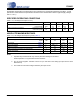
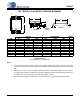
DC ELECTRICAL CHARACTERISTICS
(GND = 0 V, all voltages with respect to ground. PSR_MCLK=12.288 MHz)
Notes:
4. Power Down Mode is defined as PSR_RESET
= Low with all clocks and data lines held static.
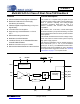
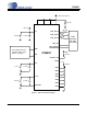
5. Valid with the recommended capacitor values on FILT+ and VQ as shown in the Typical Connection
Diagram.
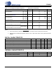
DIGITAL CHARACTERISTICS
THERMAL CHARACTERISTICS
Parameter Symbol Min Typ Max Unit
Power Supply Current VA
(Normal Operation) VDP = 5.0 V
VDP = 3.3 V
I
A
I
D
I
D
-
-
-
17.5
22
14.5
21
26
17
mA
mA
mA
Power Supply Current VA
(Power-Down Mode) (Note 4) VDP = 5.0 V
I
A
I
D
-
-
2
2
-
-
mA
mA
Power Consumption
(Normal Operation) VDP = 5.0 V
VDP = 3.3 V
(Power-Down Mode) VDP = 5.0 V
-
-
-
198
135
20
235
161
-
mW
mW
mW
mW
ADC Power Supply Rejection Ratio (1 kHz) (Note 5) PSRR - 65 - dB
V
Q
Nominal Voltage
Output Impedance
Maximum allowable DC current source/sink
-
-
-
2.5
25
0.01
-
-
-
V
kΩ
mA
FILT+ Nominal Voltage
Output Impedance
Maximum allowable DC current source/sink
-
-
-
5
18
0.01
-
-
-
V
kΩ
mA
Parameter Symbol Min Typ Max Units
High-Level Input Voltage (% of VDP) V
IH
70% - - V
Low-Level Input Voltage (% of VDP) V
IL
--30%V
High-Level Output Voltage at I
o
= 100 µA (% of VDP) V
OH
70% - - V
Low-Level Output Voltage at I
o
= 100 µA (% of VDP) V
OL
--15%V
OVERFLOW
Current Sink I
OVERFLOW
--4.0mA
Input Leakage Current I
in
--±10 µA
Parameter Symbol Min Typ Max Unit
Allowable Junction Temperature - - 135
°C
Junction to Ambient Thermal Impedance θ
JA
-70 -
°C/W