
Manual


68 DS633F1
CS44600
Power Control (address 02h)” on page 51 to a 1b. Attempts to write this register while the PDN is not set
will be ignored.
7.31 PWMOUT Delay Register (address 33h)
7.31.1 Differential Signal Delay (DIFF_DLY[2:0])
Default = 000
Function:
The Differential Signal Delay bits allow delay adjustment between each channel’s differential signals,
PWMOUTxx+ and PWMOUTxx-. This set of bits control the delay between PWMOUTxx+ and PW-
MOUTxx- across all active channels. The value of this register determines the amount of delay inserted
in the output path. The effective delay is calculated by multiplying the register value by the period of the
PWM_MCLK. This parameter can only be changed when all modulators and associated logic are in the
power-down state by setting the PDN bit in the register “Clock Configuration and Power Control (address
02h)” on page 51 to a 1b. Attempts to write this register while the PDN is not set will be ignored.
7.31.2 Channel Delay Settings (CHNL_DLY[4:0])
Default = 00000
Function:
The Channel Delay bits allow delay adjustment of each of the PWMOUT differential signal pairs, PW-
MOUTAx+/PWMOUTAx- from the associated PWMOUTBx+/PWMOUTBx-. The value of this register de-
termines the amount of delay inserted in the output path. The effective delay is calculated by multiplying
the register value by the period of the PWM_MCLK. This parameter can only be changed when all mod-
ulators and associated logic are in the power-down state by setting the PDN bit in the register “Clock Con-
figuration and Power Control (address 02h)” on page 51 to a 1b. Attempts to write this register while the
PDN is not set will be ignored.
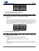
Binary Code
MIN_PULSE[4:0]
Minimum Pulse
Setting (multiply by
PWM_MCLK period)
00000 0 - no minimum
00110 6
10100 20
11111 31
Table 14. PWM Minimum Pulse Width Settings
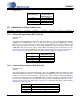
76543210
DIFF_DLY2 DIFF_DLY1 DIFF_DLY0 CHNL_DLY4 CHNL_DLY3 CHNL_DLY2 CHNL_DLY1 CHNL_DLY0
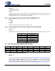
Binary Code Delay Setting (multiply by
PWM_MCLK period)
000 0 - no delay
001 1
100 4
111 7
Table 15. Differential Signal Delay Settings
Binary Code Delay Setting(multiply by PWM_MCLK period)
00000 0 - no delay
00110 6
11000 24
11111 31
Table 16. Channel Delay Settings