
Manual


DS633F1 49
CS44600
7.3 Clock Configuration and Power Control (address 02h)
7.3.1 Enable SYS_CLK Output (EN_SYS_CLK)
Default = 1
Function:
This bit enables the driver for the SYS_CLK signal. If the SYS_CLK output is unused, this bit should be
set to ‘0’b to disable the driver.
7.3.2 SYS_CLK Clock Divider Settings (SYS_CLK_DIV[1:0])
Default = 00
Function:
These two bits determine the divider for the XTAL clock signal for generating the SYS_CLK signal. During
a reset condition, with the RST
input pin held low, the logic level on the MUTE input pin will determine the
divider used for the SYS_CLK output. If MUTE
is pulled low, the SYS_CLK divider will be set to divide
the clock frequency on XTI by a factor of 1. If the MUTE
pin is pulled high, the SYS_CLK output will be
set to perform a divide-by-2 on the XTI clock. The state of the MUTE
pin will be latched on the rising edge
of the RST
. The MUTE pin can then be used as defined.
7.3.3 PWM Master Clock Divider Settings (PWM_MCLK_DIV[1:0])
Default = 00
Function:
These two bits determine the divider for the XTAL clock signal for generating the PWM_MCLK signal.
7.3.4 Power Down XTAL (PDN_XTAL)
Default = 0
0 - Crystal Oscillator Circuit is running.
1 - Crystal Oscillator Circuit is powered down.
Function:
This bit is used to power down the crystal oscillator circuitry when not being used. When using a clock
signal attached to the XTI input, this bit should be set to ‘1’b.
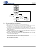
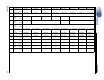
76 5 4 3 2 10
EN_SYS_CLK SYS_CLK_DIV1 SYS_CLK_DIV0 PWM_MCLK_DIV1 PWM_MCLK_DIV0 PDN_XTAL PDN_OUTPUT_MODE PDN
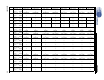
SYS_CLK_DIV[1:0] SYS_CLK Clock Divider
00 Use state of MUTE
input pin following RST
condition
01 Divide by 2
10 Divide by 4
11 Divide by 8
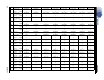
PWM_MCLK_DIV[1:0] PWM Master Clock
Divider
00 Divide by 1
01 Divide by 2
10 Divide by 4
11 Divide by 8