
Manual

8 DS792F2
CS43L22
Confidential Draft
3/4/10
1.1 I/O Pin Characteristics
Input and output levels and associated power supply voltage are shown in the table below. Logic levels
should not exceed the corresponding power supply voltage.
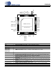
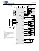
AGND 17 Analog Ground (Input) - Ground reference for the internal analog section.
FILT+ 18 Positive Voltage Reference (Output) - Filter connection for the internal sampling circuits.
VQ 19 Quiescent Voltage (Output) - Filter connection for the internal quiescent voltage.
TSTO
20,36 Test Out (Output) - This pin is an output used for test purposes only and must be left “floating” (no
connection external to the pin).
AIN4A,B
AIN3A,B
AIN2A,B
AIN1A,B
21,22
23,24
25,26
29,30
Line-Level Analog Inputs (Input) - Single-ended stereo line-level analog inputs.
AFILTA,AFILTB 27,28 Anti-alias Filter Connection (Output) - Anti-alias filter connection for analog passthrough mode.
SPKR/HP
31 Speaker/Headphone Switch (Input) - Powers down the left and/or right channel of the speaker
and/or headphone outputs.
RESET
32
Reset (Input) - The device enters a low power mode when this pin is driven low.
VL
33 Digital Interface Power (Input) - Determines the required signal level for the serial audio inter-
face and host control port.
VD 34 Digital Power (Input) - Positive power for the internal digital section.
DGND 35 Digital Ground (Input) - Ground reference for the internal digital section.
MCLK 37 Master Clock (Input) - Clock source for the delta-sigma modulators.
SCLK 38 Serial Clock (Input/Output) - Serial clock for the serial audio interface.
SDIN 39 Serial Audio Data Input (Input) - Input for two’s complement serial audio data.
LRCK
40 Left Right Clock (Input/Output) - Determines which channel, Left or Right, is currently active on
the serial audio data line.
GND/Thermal Pad
- Ground reference for PWM power FETs and charge pump; thermal relief pad for optimized heat
dissipation.
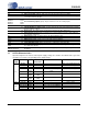
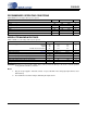
Power
Supply
Pin Name I/O Internal
Connections
Driver Receiver
VL
RESET Input - - 1.65 V - 3.47 V, with Hysteresis
AD0 Input - - 1.65 V - 3.47 V, with Hysteresis
SCL Input - - 1.65 V - 3.47 V, with Hysteresis
SDA Input/
Output
- 1.65 V - 3.47 V, CMOS/Open
Drain
1.65 V - 3.47 V, with Hysteresis
MCLK Input - - 1.65 V - 3.47 V
LRCK Input/
Output
Weak Pull-up
(~1 MΩ)
1.65 V - 3.47 V, CMOS 1.65 V - 3.47 V
SCLK Input/
Output
Weak Pull-up
(~1 MΩ)
1.65 V - 3.47 V, CMOS 1.65 V - 3.47 V
SDIN Input - - 1.65 V - 3.47 V
VA SPKR/HP Input - - 1.65 V - 2.63 V
VP
SPKR_OUTA+ Output - 1.6 V - 5.25 V Power MOSFET -
SPKR_OUTA- Output - 1.6 V - 5.25 V Power MOSFET -
SPKR_OUTB+ Output - 1.6 V - 5.25 V Power MOSFET -
SPKR_OUTB- Output - 1.6 V - 5.25 V Power MOSFET -