
Manual


14 DS792F2
CS43L22
Confidential Draft
3/4/10
6. The PWM driver should be used in captive speaker systems only.
7. Optimal PWM performance is achieved when MCLK > 12 MHz.
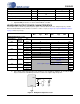
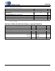
HEADPHONE OUTPUT POWER CHARACTERISTICS
Test conditions (unless otherwise specified): Input test signal is a full-scale 997 Hz sine wave; Sample Frequency = 48 kHz;
Measurement Bandwidth is 20 Hz to 20 kHz; Test load R
L
= 16 Ω, C
L
= 10 pF (see Figure 2); “Required Initialization Settings”
on page 32 written on power up.
8. VHP settings lower than VA reduces the headroom of the headphone amplifier. As a result, the DAC
may not achieve the full THD+N performance at full-scale output voltage and power.
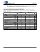
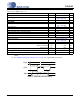
MOSFET On Resistance R
DS(ON)
VP = 2.5V, I
d
= 0.5 A - 760 - mΩ
Efficiency η VP = 5.0 V, P
O
= 2 x 0.8 W, R
L
=
8 Ω
-81-%
Output Operating Peak Current I
PC
--1.5A
VP Input Current During Reset I
VP
RESET, pin 32, is held low
-0.85.0µA
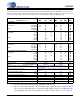
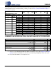
Parameters VA = 2.5V
Min Typ Max
VA = 1.8V
Min Typ Max
Unit
AOUTx Power Into R
L
= 16
Ω
HP_GAIN[2:0] Analog
Gain (G)
VHP
000 0.3959 1.8 V - 14 - - 7 - mW
rms
2.5 V - 14 - - 7 - mW
rms
001 0.4571 1.8 V - 19 - - 10 - mW
rms
2.5 V - 19 - - 10 - mW
rms
010 0.5111 1.8 V - 23 - - 12 - mW
rms
2.5 V - 23 - - 12 - mW
rms
011 (default) 0.6047 1.8 V (Note 8) - 17 - mW
rms
2.5 V - 32 - - 17 - mW
rms
100 0.7099 1.8 V (Note 8) - 23 - mW
rms
2.5 V - 44 - - 23 - mW
rms
101 0.8399 1.8 V (Note 4) See Figure 18 on
page 59
mW
rms
2.5 V - 32 - mW
rms
110 1.0000 1.8 V (Note 4, 8) See Figures 18 and 19 on page 59 mW
rms
2.5 V mW
rms
111 1.1430 1.8 V mW
rms
2.5 V mW
rms
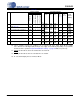
Parameters (Note 7) Symbol Conditions Min Typ Max Units
AOUTx
AGND
R
L
C
L
0.022 μF
51 Ω
Figure 2. Headphone Output Test Load