Confidential Draft 3/4/10 CS43L22 Low Power, Stereo DAC w/Headphone & Speaker Amps FEATURES Class D Stereo/Mono Speaker Amplifier 98 dB Dynamic Range (A-wtd) No External Filter Required 88 dB THD+N Headphone Amplifier - GND Centered – No DC-Blocking Capacitors Required – Integrated Negative Voltage Regulator – 2 x 23 mW into Stereo 16 Ω @ 1.8 V – 2 x 44 mW into Stereo 16 Ω @ 2.
Confidential Draft 3/4/10 CS43L22 System Features General Description 12, 24, and 27 MHz Master Clock Support in The CS43L22 is a highly integrated, low power stereo DAC with headphone and Class D speaker amplifiers. The CS43L22 offers many features suitable for low power, portable system applications.
Confidential Draft 3/4/10 CS43L22 TABLE OF CONTENTS 1. PIN DESCRIPTIONS .............................................................................................................................. 7 1.1 I/O Pin Characteristics ..................................................................................................................... 8 2. TYPICAL CONNECTION DIAGRAM ..................................................................................................... 9 3.
Confidential Draft 3/4/10 CS43L22 7.2.1 Power Down .......................................................................................................................... 37 7.3 Power Control 2 (Address 04h) ...................................................................................................... 38 7.3.1 Headphone Power Control .................................................................................................... 38 7.3.2 Speaker Power Control ...............................
Confidential Draft 3/4/10 CS43L22 7.16 Beep Volume & Off Time (Address 1Dh) ..................................................................................... 48 7.16.1 Beep Off Time ..................................................................................................................... 48 7.16.2 Beep Volume ....................................................................................................................... 49 7.17 Beep & Tone Configuration (Address 1Eh) ................
Confidential Draft 3/4/10 CS43L22 11. DIGITAL FILTER PLOTS ................................................................................................................... 63 12. PARAMETER DEFINITIONS .............................................................................................................. 64 13. PACKAGE DIMENSIONS .................................................................................................................. 65 THERMAL CHARACTERISTICS ...........................
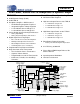
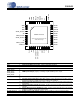
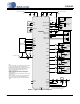
Confidential Draft 3/4/10 CS43L22 TSTO DGND VD VL RESET SPKR/HP 36 35 34 33 32 31 MCLK 37 SDIN SCLK 39 38 LRCK SDA 1 30 AIN1B SCL 2 29 AIN1A AD0 3 28 AFILTB SPKR_OUTA+ 4 27 AFILTA VP 5 26 AIN2B SPKR_OUTA- 6 25 AIN2A SPKR_OUTB+ 7 24 AIN3B VP 8 23 AIN3A SPKR_OUTB- 9 22 AIN4B -VHPFILT 10 21 AIN4A Pin Name SDA SCL AD0 SPKR_OUTA+ SPKR_OUTASPKR_OUTB+ SPKR_OUTBVP -VHPFILT FLYN FLYP +VHP HP/LINE_OUTB, A VA DS792F2 40 1.
Confidential Draft 3/4/10 AGND FILT+ VQ 17 18 19 20,36 TSTO AIN4A,B AIN3A,B AIN2A,B AIN1A,B AFILTA,AFILTB SPKR/HP RESET VL VD DGND MCLK SCLK SDIN LRCK GND/Thermal Pad 1.1 CS43L22 Analog Ground (Input) - Ground reference for the internal analog section. Positive Voltage Reference (Output) - Filter connection for the internal sampling circuits. Quiescent Voltage (Output) - Filter connection for the internal quiescent voltage.
Confidential Draft 3/4/10 CS43L22 2. TYPICAL CONNECTION DIAGRAM +1.8 V to +2.5 V +1.8 V to +2.5 V 1 µF 0.1 µF 0.1 µF 0.1 µF VD VA 1 µF See Note 4 +VHP Line Level Out Left & Right 47 kΩ 0.022 µF Note 1 1 µF ** FLYP HP/LINE_OUTB FLYN HP/LINE_OUTA Headphone Out Left & Right 51.1 Ω 0.022 µF Note 2 -VHPFILT 1 µF 51.1 Ω SPKR/HP ** CS43L22 VP 0.1 µF 10 µF +1.6 V to Stereo Speakers +5 V SPKR_OUTA+ SPKR_OUTAVP 0.
Confidential Draft 3/4/10 CS43L22 3. CHARACTERISTIC AND SPECIFICATIONS RECOMMENDED OPERATING CONDITIONS AGND=DGND=0 V, all voltages with respect to ground. Parameters DC Power Supply Analog Headphone Amplifier Speaker Amplifier Digital Serial/Control Port Interface Ambient Temperature Commercial Symbol Min Max Units VA +VHP VP VD VL TA 1.65 1.65 1.60 1.65 1.65 -40 2.63 2.63 5.25 2.63 3.47 +85 V V V V V °C ABSOLUTE MAXIMUM RATINGS AGND = DGND = 0 V; all voltages with respect to ground.
Confidential Draft 3/4/10 CS43L22 ANALOG OUTPUT CHARACTERISTICS Test conditions (unless otherwise specified): Input test signal is a full-scale 997 Hz sine wave; All Supplies = VA; TA = +25°C; Sample Frequency = 48 kHz; Measurement bandwidth is 20 Hz to 20 kHz; Test load RL = 10 kΩ, CL = 10 pF for the line output (see Figure 2); Test load RL = 16 Ω, CL = 10 pF (see Figure 2) for the headphone output; HP_GAIN[2:0] = 011. VA = 2.5 V Min Typ Max Parameters (Note 3) VA = 1.
Confidential Draft 3/4/10 CS43L22 5. See Figure 2. RL and CL reflect the recommended minimum resistance and maximum capacitance required for the internal op-amp's stability and signal integrity. In this circuit topology, CL will effectively move the band-limiting pole of the amp in the output stage. Increasing this value beyond the recommended 150 pF can cause the internal op-amp to become unstable.
Confidential Draft 3/4/10 CS43L22 PWM OUTPUT CHARACTERISTICS Test conditions (unless otherwise specified): Input test signal is a full scale 997 Hz signal; MCLK = 12.2880 MHz; Measurement Bandwidth is 20 Hz to 20 kHz; Sample Frequency = 48 kHz; Test load RL = 8 Ω for stereo full-bridge, RL = 4 Ω for mono parallel full-bridge; VD = VL = VA = VHP = 1.8V; PWM Modulation Index of 0.85; PWM Switch Rate = 384 kHz. Parameters (Note 7) Symbol VP = 5.
Confidential Draft 3/4/10 Parameters (Note 7) MOSFET On Resistance Efficiency CS43L22 Symbol Conditions Min Typ Max Units RDS(ON) η VP = 2.5V, Id = 0.5 A VP = 5.0 V, PO = 2 x 0.8 W, RL = 8Ω - 760 81 - mΩ % - 0.8 1.5 5.0 A µA Output Operating Peak Current VP Input Current During Reset IPC IVP RESET, pin 32, is held low 6. The PWM driver should be used in captive speaker systems only. 7. Optimal PWM performance is achieved when MCLK > 12 MHz.
Confidential Draft 3/4/10 CS43L22 LINE OUTPUT VOLTAGE LEVEL CHARACTERISTICS Test conditions (unless otherwise specified): Input test signal is a full-scale 997 Hz sine wave; measurement bandwidth is 20 Hz to 20 kHz; Sample Frequency = 48 kHz; Test load RL = 10 kΩ, CL = 10 pF (see Figure 2); “Required Initialization Settings” on page 32 written on power up. Parameters Min VA = 2.5V Typ Max Min 2.15 - 1.41 - - - VA = 1.
Confidential Draft 3/4/10 CS43L22 SWITCHING SPECIFICATIONS - SERIAL PORT Inputs: Logic 0 = DGND; Logic 1 = VL. Parameters Symbol RESET pin Low Pulse Width MCLK Frequency (Note 12) (Note 11) MCLK Duty Cycle Min Max 1 - Units ms (See “Serial Port Clocking” on page 29) 45 55 MHz (See “Serial Port Clocking” on page 29) 45 55 64•Fs 45 55 40 20 20 - kHz (See “Serial Port Clocking” on page 29) 45 55 12.
Confidential Draft 3/4/10 CS43L22 SWITCHING SPECIFICATIONS - I²C CONTROL PORT Inputs: Logic 0 = DGND; Logic 1 = V; SDA CL = 30 pF. Parameters Symbol Min Max Unit SCL Clock Frequency fscl - 100 kHz RESET Rising Edge to Start tirs 550 - ns Bus Free Time Between Transmissions tbuf 4.7 - µs Start Condition Hold Time (prior to first clock pulse) thdst 4.0 - µs Clock Low time tlow 4.7 - µs Clock High Time thigh 4.0 - µs Setup Time for Repeated Start Condition tsust 4.
Confidential Draft 3/4/10 CS43L22 DC ELECTRICAL CHARACTERISTICS AGND = 0 V; all voltages with respect to ground. Parameters Min Typ Max Units - 0.5•VA 23 - 1 V kΩ μA VQ Characteristics Nominal Voltage Output Impedance DC Current Source/Sink Power Supply Rejection Ratio Characteristics PSRR @ 1 kHz (Note 14) DAC (HP & Line Amps) - 60 - dB PSRR @ 60 Hz (Note 14) DAC (HP & Line Amps) - 60 - dB Full-Bridge PWM Outputs - 56 - dB PSRR @ 217 Hz 14.
Confidential Draft 3/4/10 CS43L22 POWER CONSUMPTION See (Note 16) PDN_HPA[1:0] PDN_SPKB[1:0] PDN_SPKA[1:0] Typical Current (mA) PDN_HPB[1:0] Register Settings 02h 04h PDN[7:0] Operation x x x x x Standby (Note 18) 0x9F x x 3 Stereo Passthrough to Headphone 0x9E 10 10 4 Mono Playback to Headphone 0x9E 10 11 5 Stereo Playback to Headphone 0x9E 10 10 6 Mono Playback to Speaker 0x9E 11 11 7 Stereo Playback to Speaker 0x9E 11 11 1 Off (Note 17) 2 iVHP iVA iVD iVL iVP V
Confidential Draft 3/4/10 CS43L22 4. APPLICATIONS 4.1 4.1.1 Overview Basic Architecture The CS43L22 is a highly integrated, low power, 24-bit audio DAC comprised of a Digital Signal Processing Engine, headphone amplifiers, a digital PWM modulator and two full-bridge power back-ends. Other features include battery level monitoring and compensation and temperature monitoring.
Confidential Draft 3/4/10 4.2 CS43L22 DSP Engine Fixed Function DSP LIMARATE[7:0] LIMRRATE[7:0] LMAX[2:0] CUSH[2:0] LIMSRDIS LIMZCDIS LIMIT MSTAVOL[7:0] MSTBVOL[7:0] +12dB/-102dB 0.5dB steps PCM Serial Interface Chnl Vol. Settings Limiter PWM Modulator PCMAMUTE PCMBMUTE PCMAVOL[6:0] PCMBVOL[6:0] +12dB/-51.5dB 0.
Confidential Draft 3/4/10 4.2.1 CS43L22 Beep Generator The Beep Generator generates audio frequencies across approximately two octave major scales. It offers three modes of operation: Continuous, multiple and single (one-shot) beeps. Sixteen on and eight off times are available. Note: The Beep is generated before the limiter and may affect desired limiting performance.
Confidential Draft 3/4/10 CS43L22 the thresholds. Referenced Control Register Location Limiter Controls ................... “Limiter Control 2, Release Rate (Address 28h)” on page 54, “Limiter Attack Rate (Address 29h)” on page 55 Master Volume Control........
Confidential Draft 3/4/10 4.3 CS43L22 Analog Passthrough The CS43L22 accommodates analog routing of the analog input signal directly to the headphone amplifiers by using the PASSTHRUx mux. This feature is useful in applications that utilize an FM tuner where audio recovered over-the-air must be transmitted to the headphone amplifier directly. This analog passthrough path reduces power consumption and is immune to modulator switching noise that could interfere with some tuners.
Confidential Draft 3/4/10 4.4 CS43L22 Analog Outputs PDN_HPA[1:0] PDN_HPB[1:0] HPAMUTE HPBMUTE HPA_VOL[7:0] HPB_VOL[7:0] +0dB/-102dB 0.5dB steps from DSP Engine HPGAIN[2:0] A DAC VOL HP/Line Outputs B Analog Passthru Input Signal Charge Pump VOL PASSTHRUA PASSTHRUB PASSAMUTE PASSBMUTE PASSAVOL[7:0] PASSBVOL[70] +12dB/-60dB 0.5dB steps CHGFREQ[3:0] Figure 9. Analog Outputs Referenced Control Register Location Analog Output HPxMUTE ........................... HPxVOL[7:0] .......................
Confidential Draft 3/4/10 4.5 CS43L22 PWM Outputs Note: The PWM speaker amplifiers should not be used in the 384x MCLK modes (18.4320 and 16.9344 MHz). SPKAMUTE SPKBMUTE MUTE50/50 SPKMONO SPKSWAP SPKB=A SPKAVOL[7:0] SPKBVOL[7:0] +0dB/-102dB 0.5dB steps from DSP Engine BATTCMP VPREF[3:0] VPLVL[7:0] Battery Compensation PWM Modulator VOL + A + B - Gate Drive Speaker Outputs PDN_SPKA[1:0] PDN_SPKB[1:0] Short Circuit SPKASHRT SPKBSHRT Figure 10.
Confidential Draft 3/4/10 4.5.1 CS43L22 Mono Speaker Output Configuration The CS43L22 accommodates a stereo as well as a mono speaker output configuration. In mono mode the output drivers of each channel are connected in parallel to deliver maximum power to a 4 ohm speaker. Refer to the table below for pin mapping in mono configuration.
Confidential Draft 3/4/10 CS43L22 -6 Battery Compensated PWM Output Level PWM Output Level (dB) -8 -10 -12 Uncompensated PWM Output Level -14 -16 -18 -20 -22 -24 4.9 4.6 4.3 4 3.7 3.4 3.1 2.8 2.5 2.2 1.9 1.6 VP Supply (V) Figure 11. Battery Compensation 28 Referenced Control Register Location VPREF ................................ SPKxVOL ............................
Confidential Draft 3/4/10 4.6 CS43L22 Serial Port Clocking The CS43L22 serial audio interface port operates either as a slave or master, determined by the M/S bit. It accepts externally generated clocks in Slave Mode and will generate synchronous clocks derived from an input master clock (MCLK) in Master Mode. Refer to the tables below for the required setting in register 05h and 06h associated with a given MCLK and sample rate. Referenced Control Register Location M/S...................................
Confidential Draft 3/4/10 MCLK (MHz) Sample Rate, Fs (kHz) 8.0000 12.0000 24.0000 32.0000 *44.1176... 48.0000 *11.0294... *22.0588... 16.0000 27.0000 Note: SPEED[1:0] (AUTO=’0’b) 11 11 10 01 01 01 11 10 10 CS43L22 32kGROUP VIDEOCLK RATIO[1:0] MCLKDIV2 1 0 0 1 0 0 0 0 1 1 1 1 1 1 1 1 1 1 01 01 01 01 11 01 11 11 01 0 0 0 0 0 0 0 0 0 *The marked sample rate values are not exact representations of the actual frame clock frequency They have been truncated to 4 decimal places.
Confidential Draft 3/4/10 4.7.1 CS43L22 DSP Mode In DSP Mode, the LRCK acts as a frame sync for 2 data-packed words (left and right channel) input on SDIN. The MSB is input on the first SCLK rising edge after the frame sync rising edge. The right channel immediately follows the left channel. 1/fs LRCK SCLK SDIN L SB MSB L eft C h a n n el LS B M SB HP/LINE OUTA R ig ht C h a n n el LSB M SB HP/LINE OUTB Audio Word Length (AWL) Figure 15. DSP Mode Format) 4.
Confidential Draft 3/4/10 CS43L22 4. Wait at least 100 µs. The device will be fully powered down after this 100 µs delay. Prior to the removal of the master clock (MCLK), this delay of at least 100 µs must be implemented after step 3 to avoid premature disruption of the DAC’s power down sequence. A disruption in the device’s power down sequence (i.e.
Confidential Draft 3/4/10 CS43L22 5. CONTROL PORT OPERATION The control port is used to access the registers allowing the CS43L22 to be configured for the desired operational modes and formats. The operation of the control port may be completely asynchronous with respect to the audio sample rates. However, to avoid potential interference problems, the control port pins should remain static if no operation is required.
Confidential Draft 3/4/10 CS43L22 Send start condition. Send 10010100 (chip address & write operation). Receive acknowledge bit. Send MAP byte, auto-increment off. Receive acknowledge bit. Send stop condition, aborting write. Send start condition. Send 10010101 (chip address & read operation). Receive acknowledge bit. Receive byte, contents of selected register. Send acknowledge bit. Send stop condition. Setting the auto-increment bit in the MAP allows successive reads or writes of consecutive registers.
Confidential Draft 3/4/10 CS43L22 6. REGISTER QUICK REFERENCE Default values are shown below the bit names. Unless otherwise specified, all “Reserved” bits must maintain their default value. Adr.
Confidential Draft 3/4/10 Adr.
Confidential Draft 3/4/10 CS43L22 7. REGISTER DESCRIPTION All registers are read/write except for the chip I.D. and Revision Register and Interrupt Status Register which are read only. See the following bit definition tables for bit assignment information. The default state of each bit after a power-up sequence or reset is shown as shaded in the table. Unless otherwise specified, all “Reserved” bits must maintain their default value. 7.1 Chip I.D.
Confidential Draft 3/4/10 7.3 CS43L22 Power Control 2 (Address 04h) 7 PDN_HPB1 7.3.1 6 PDN_HPB0 5 PDN_HPA1 4 PDN_HPA0 3 PDN_SPKB1 2 PDN_SPKB0 1 PDN_SPKA1 0 PDN_SPKA0 Headphone Power Control Configures how the SPK/HP_SW pin, 6, controls the power for the headphone amplifier. 7.3.2 PDN_HPx[1:0] Headphone Status 00 Headphone channel is ON when the SPK/HP_SW pin, 6, is LO. Headphone channel is OFF when the SPK/HP_SW pin, 6, is HI. 01 Headphone channel is ON when the SPK/HP_SW pin, 6, is HI.
Confidential Draft 3/4/10 7.4.2 CS43L22 Speed Mode Configures the speed mode of the DAC in Slave Mode and sets the appropriate MCLK divide ratio for LRCK and SCLK in Master Mode. SPEED[1:0] Slave Mode Master Mode Serial Port Speed MCLK/LRCK Ratio SCLK/LRCK Ratio 00 Double-Speed Mode (DSM - 50 kHz -100 kHz Fs) 512 64 01 Single-Speed Mode (SSM - 4 kHz -50 kHz Fs) 256 64 10 Half-Speed Mode (HSM - 12.5kHz -25 kHz Fs) 128 64 11 Quarter-Speed Mode (QSM - 4 kHz -12.
Confidential Draft 3/4/10 7.4.6 CS43L22 MCLK Divide By 2 Divides the input MCLK by 2 prior to all internal circuitry. MCLKDIV2 No divide 1 Divided by 2 Application: “Serial Port Clocking” on page 29 Note: 7.5 MCLK signal into DAC 0 In Slave Mode, this bit is ignored when the AUTO bit (“Auto-Detect” on page 38) is disabled. Interface Control 1 (Address 06h) 7 M/S 7.5.
Confidential Draft 3/4/10 7.5.5 CS43L22 Audio Word Length Configures the audio sample word length used for the data into SDIN. Audio Word Length AWL[1:0] DSP Mode Right Justified 00 32-bit data 24-bit data 01 24-bit data 20-bit data 10 20-bit data 18-bit data 11 16-bit data 16-bit data Application: “DSP Mode” on page 31 Note: When the internal MCLK/LRCK ratio is set to 125 in Master Mode, the 32-bit data width option for DSP Mode is not valid unless SCLK=MCLK. 7.
Confidential Draft 3/4/10 7.7 Passthrough x Select: PassA (Address 08h), PassB (Address 09h) 7 Reserved 7.7.1 CS43L22 6 Reserved 5 Reserved 4 Reserved 3 2 1 0 PASSASEL4 PASSASEL3 PASSASEL2 PASSASEL1 Passthrough Input Channel Mapping Selects one or sums/mixes the analog input signal into the passthrough Amplifier. Each bit of the PASSx_SEL[4:1] word corresponds to individual channels (i.e. PASSx_SEL1 selects AIN1x, PASSx_SEL2 selects AIN2x, etc.).
Confidential Draft 3/4/10 7.10 CS43L22 Playback Control 1 (Address 0Dh) 7 HPGAIN2 6 HPGAIN1 5 HPGAIN0 4 PLYBCKB=A 3 INV_PCMB 2 INV_PCMA 1 MSTBMUTE 0 MSTAMUTE 7.10.1 Headphone Analog Gain Selects the gain multiplier for the headphone/line outputs. HPGAIN[2:0] Headphone/Line Gain Setting (G) 000 0.3959 001 0.4571 010 0.5111 011 0.6047 100 0.7099 101 0.8399 110 1.000 111 1.
Confidential Draft 3/4/10 7.11 Miscellaneous Controls (Address 0Eh) 7 6 5 4 PASSTHRUB PASSTHRUA PASSBMUTE PASSAMUTE 7.11.1 CS43L22 3 FREEZE 2 DEEMPH 1 DIGSFT 0 DIGZC Passthrough Analog Configures an analog passthrough from the analog inputs to the headphone/line outputs. PASSTHRUx 7.11.2 Analog In Routed to HP/Line Output 0 Disabled 1 Enabled Passthrough Mute Configures an analog mute on the channel x analog in to analog out passthrough. PASSxMUTE 7.11.
Confidential Draft 3/4/10 7.11.6 CS43L22 Digital Zero Cross Configures when the signal level changes occur for the digital volume controls.
Confidential Draft 3/4/10 CS43L22 7.12.5 Speaker MONO Control Configures a parallel full bridge output for the speaker channels. SPKMONO Parallel Full Bridge Output 0 Disabled 1 Enabled Application: “Mono Speaker Output Configuration” on page 27 7.12.6 Speaker Mute 50/50 Control Configures how the speaker channels mute. 7.13 MUTE50/50 Speaker Mute 50/50 0 Disabled; The PWM amplifiers outputs modulated silence when SPKxMUTE is enabled.
Confidential Draft 3/4/10 7.14 CS43L22 PCMx Volume: PCMA (Address 1Ah) & PCMB (Address 1Bh) 7 PCMxMUTE 6 PCMxVOL6 5 PCMxVOL5 4 PCMxVOL4 3 PCMxVOL3 2 PCMxVOL2 1 PCMxVOL1 0 PCMxVOL0 7.14.1 PCM Channel x Mute Configures a digital mute on the PCM data from the serial data input (SDIN) to the DSP. PCMxMUTE PCM Mute 0 Disabled 1 Enabled 7.14.2 PCM Channel x Volume Sets the volume/gain of the PCM data from the serial data input (SDIN) to the DSP. 7.15 PCMxVOL[6:0] Volume 001 1000 +12.0 dB ..
Confidential Draft 3/4/10 CS43L22 Notes: 1. This setting must not change when BEEP is enabled. 2. Beep frequency will scale directly with sample rate, Fs, but is fixed at the nominal Fs within each speed mode. 7.15.2 Beep On Time Sets the on duration of the beep signal. ONTIME[3:0] On Time (Fs = 12, 24, 48 or 96 kHz) 0000 ~86 ms 0001 ~430 ms 0010 ~780 ms 0011 ~1.20 s 0100 ~1.50 s 0101 ~1.80 s 0110 ~2.20 s 0111 ~2.50 s 1000 ~2.80 s 1001 ~3.20 s 1010 ~3.50 s 1011 ~3.80 s 1100 ~4.
Confidential Draft 3/4/10 CS43L22 Notes: 1. This setting must not change when BEEP is enabled. 2. Beep off time will scale inversely with sample rate, Fs, but is fixed at the nominal Fs within each speed mode. 7.16.2 Beep Volume Sets the volume of the beep signal. BEEPVOL[4:0] Gain 00110 +6.0 dB ··· ··· 00000 -6 dB 11111 -8 dB 11110 -10 dB ··· ··· 00111 -56 dB Step Size: 2 dB Application: “Beep Generator” on page 22 Note: 7.17 This setting must not change when BEEP is enabled.
Confidential Draft 3/4/10 CS43L22 7.17.3 Treble Corner Frequency Sets the corner frequency (-3 dB point) for the treble shelving filter. TREBCF[1:0] Treble Corner Frequency Setting 00 5 kHz 01 7 kHz 10 10 kHz 11 15 kHz 7.17.4 Bass Corner Frequency Sets the corner frequency (-3 dB point) for the bass shelving filter. BASSCF[1:0] Bass Corner Frequency Setting 00 50 Hz 01 100 Hz 10 200 Hz 11 250 Hz 7.17.5 Tone Control Enable Configures the treble and bass activation. 7.
Confidential Draft 3/4/10 CS43L22 7.18.2 Bass Gain Sets the gain of the bass shelving filter. 7.19 TREB[3:0] Gain Setting 0000 +12.0 dB ··· ··· 0111 +1.5 dB 1000 0 dB 1001 -1.5 dB ··· ··· 1111 -10.5 dB Step Size: 1.5 dB Master Volume Control: MSTA (Address 20h) & MSTB (Address 21h) 7 MSTxVOL7 6 MSTxVOL6 5 MSTxVOL5 4 MSTxVOL4 3 MSTxVOL3 2 MSTxVOL2 1 MSTxVOL1 0 MSTxVOL0 7.19.1 Master Volume Control Sets the volume of the signal out the DSP. 7.
Confidential Draft 3/4/10 7.21 CS43L22 Speaker Volume Control: SPKA (Address 24h) & SPKB (Address 25h) 7 SPKxVOL7 6 SPKxVOL6 5 SPKxVOL5 4 SPKxVOL4 3 SPKxVOL3 2 SPKxVOL2 1 SPKxVOL1 0 SPKxVOL0 2 Reserved 1 Reserved 0 Reserved 7.21.1 Speaker Volume Control Sets the volume of the signal out the PWM modulator. SPKxVOL[7:0] 0 dB 1111 1111 -0.5 dB 1111 1110 -1.0 dB ··· ··· 0100 0000 -96.0 dB ··· ··· 0000 0001 Muted Step Size: 0.5 dB Note: 7.
Confidential Draft 3/4/10 7.23 CS43L22 Limiter Control 1, Min/Max Thresholds (Address 27h) 7 LMAX2 6 LMAX1 5 LMAX0 4 CUSH2 3 CUSH1 2 CUSH0 1 LIMSRDIS 0 LIMZCDIS 7.23.1 Limiter Maximum Threshold Sets the maximum level, below full scale, at which to limit and attenuate the output signal at the attack rate (LIMARATE - “Limiter Release Rate” on page 54).
Confidential Draft 3/4/10 CS43L22 7.23.4 Limiter Zero Cross Disable Configures an override of the digital zero cross setting. 7.24 LIMZCDIS Limiter Zero Cross Disable 0 OFF; Limiter Attack Rate is dictated by the DIGZC (“Digital Zero Cross” on page 45) setting 1 ON; Limiter volume changes take effect in one step, regardless of the DIGZC setting.
Confidential Draft 3/4/10 7.25 CS43L22 Limiter Attack Rate (Address 29h) 7 Reserved 6 Reserved 5 LIMARATE5 4 LIMARATE4 3 LIMARATE3 2 LIMARATE2 1 LIMARATE1 0 LIMARATE0 7.25.1 Limiter Attack Rate Sets the rate at which the limiter applies digital attenuation from levels above the MAX[2:0] threshold (“Limiter Maximum Threshold” on page 53).
Confidential Draft 3/4/10 CS43L22 7.26.3 PCMx Overflow (Read Only) Indicates the over-range status in the PCM data path. 7.27 PCMxOVFL PCM Overflow Status: 0 No digital clipping has occurred in the data path of the PCM (“PCM Channel x Volume” on page 47) of the DSP. 1 Digital clipping has occurred in the data path of the PCM of the DSP.
Confidential Draft 3/4/10 CS43L22 7.27.3 VP Reference Sets the desired VP reference used for battery compensation. VPREF[3:0] Desired VP used to calculate the required attenuation on the speaker output: 0000 1.5 V 0001 2.0 V (for VA = 1.8 V) 0010 2.5 V 0011 3.0 V 0100 3.5 V 0101 4.0 V 0110 4.5 V 0111 5.0 V 1000 1.5 V 1001 2.0 V (for VA = 2.5 V) 7.28 1010 2.5 V 1011 3.0 V 1100 3.5 V 1101 4.0 V 1110 4.5 V 1111 5.
Confidential Draft 3/4/10 CS43L22 7.29.2 SPKR/HP Pin Status (Read Only) Indicates the status of the SPKR/HP pin. 7.30 SPKR/HP Pin State 0 Pulled Low 1 Pulled High Charge Pump Frequency (Address 34h) 7 CHGFREQ3 6 CHGFREQ2 5 CHGFREQ1 4 CHGFREQ0 3 Reserved 2 Reserved 1 Reserved 0 Reserved 7.30.1 Charge Pump Frequency Sets the charge pump frequency on FLYN and FLYP. CHGFREQ[3:0] N 0000 0 ... 0101 5 ...
Confidential Draft 3/4/10 CS43L22 8. ANALOG PERFORMANCE PLOTS 8.1 Headphone THD+N versus Output Power Plots Test conditions (unless otherwise specified): Input test signal is a 997 Hz sine wave; measurement bandwidth is 10 Hz to 20 kHz; Fs = 48 kHz. -10 G = 0.6047 -15 VHP = VA = 1.8 V G = 0.7099 -20 G = 0.8399 -25 -30 G = 1.0000 -35 G = 1.1430 -40 Legend -45 d B r A -50 NOTE: Graph shows the output power per channel (i.e.
Confidential Draft 3/4/10 CS43L22 G = 0.6047 VHP = VA = 1.8 V G = 0.7099 -20 -30 G = 0.8399 -35 G = 1.0000 -40 G = 1.1430 -45 Legend -50 NOTE: Graph shows the output power per channel (i.e. Output Power = 22 mW into single 32 Ω and 44 mW into stereo 32 Ω with THD+N = 75 dB). -55 d B r -60 A -65 -70 -75 -80 -85 -90 -95 -100 0 6m 12m 18m 24m 30m 36m 42m 48m 54m 60m W Figure 20. THD+N vs. Output Power per Channel at 1.8 V (32 Ω load) G = 0.6047 -20 VHP = VA = 2.
Confidential Draft 3/4/10 9. EXAMPLE SYSTEM CLOCK FREQUENCIES 9.1 9.2 CS43L22 *The”MCLKDIV2” bit must be enabled. Auto Detect Enabled Sample Rate LRCK (kHz) 1024x MCLK (MHz) 1536x 2048x* 8 11.025 12 3072x* 8.1920 11.2896 12.2880 12.2880 16.9344 18.4320 24.5760 33.8688 36.8640 Sample Rate LRCK (kHz) 512x MCLK (MHz) 768x 1024x* 16 22.05 24 8.1920 11.2896 12.2880 Sample Rate LRCK (kHz) 256x 32 44.1 48 8.1920 11.2896 12.2880 Sample Rate LRCK (kHz) 128x 64 88.2 96 8.1920 11.2896 12.
Confidential Draft 3/4/10 CS43L22 10.PCB LAYOUT CONSIDERATIONS 10.1 Power Supply, Grounding As with any high-resolution converter, the CS43L22 requires careful attention to power supply and grounding arrangements if its potential performance is to be realized. Figure 1 on page 9 shows the recommended power arrangements, with VA and VHP connected to clean supplies VD, which powers the digital circuitry, may be run from the system logic supply.
Confidential Draft 3/4/10 CS43L22 11.DIGITAL FILTER PLOTS DS792F2 Figure 22. Passband Ripple Figure 23. Stopband Figure 24. DAC Transition Band Figure 25.
Confidential Draft 3/4/10 CS43L22 12.PARAMETER DEFINITIONS Dynamic Range The ratio of the rms value of the signal to the rms sum of all other spectral components over the specified bandwidth. Dynamic Range is a signal-to-noise ratio measurement over the specified band width made with a -60 dBFS signal. 60 dB is added to resulting measurement to refer the measurement to full-scale. This technique ensures that the distortion components are below the noise level and do not affect the measurement.
Confidential Draft 3/4/10 CS43L22 13.PACKAGE DIMENSIONS 40L QFN (6 X 6 mm BODY) PACKAGE DRAWING D b 2.00REF e PIN #1CORNER 2.00REF PIN #1IDENTIFIER ∅0.50±0.10 LASER MARKING E2 E A1 L D2 A DIM A A1 b D D2 E E2 e L MIN -0.0000 0.0071 0.1594 0.1594 0.0118 INCHES NOM --0.0091 0.2362 BSC 0.1614 0.2362 BSC 0.1614 0.0197 BSC 0.0157 MAX 0.0394 0.0020 0.0110 MIN -0.00 0.18 0.1634 4.05 0.1634 4.05 0.0197 0.30 MILLIMETERS NOM --0.23 6.00 BSC 4.10 6.00 BSC 4.10 0.50 BSC 0.40 NOTE MAX 1.00 0.
Confidential Draft 3/4/10 CS43L22 14.ORDERING INFORMATION Product Description Low-Power Stereo DAC CS43L22 w/HP and Speaker Amps for Portable Apps CS43L22 Evaluation CDB43L22 Board Package Pb-Free 40L-QFN Yes - No Grade Temp Range Commercial -40 to +85° C - Container Order # Rail CS43L22-CNZ Tape & Reel CS43L22-CNZR - - CDB43L22 15.REFERENCES 1. Philips Semiconductor, The I²C-Bus Specification: Version 2.1, January 2000. http://www.semiconductors.philips.com 16.