
Instruction Manual


DS723F1 31
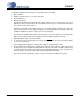
CS43L21
4.6 Initialization
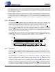
The initialization and Power-Down sequence flowchart is shown in Figure 16 on page 31. The device enters
a Power-Down state upon initial power-up. The interpolation and decimation filters, delta-sigma modulators
and control port registers are reset. The internal voltage reference, multi-bit DAC and switched-capacitor
low-pass filters are powered down.
The device will remain in the Power-Down state until the RESET
pin is brought high. The control port is ac-
cessible once RESET
is high and the desired register settings can be loaded per the interface descriptions
in “Software Mode” on page 34. If a valid write sequence to the control port is not made within approximately
10 ms, the device will enter Hardware Mode.
Once MCLK is valid, the quiescent voltage, VQ, and the internal voltage reference, FILT+ will begin powering
up to normal operation. The charge pump slowly powers up and charges the capacitors. Power is then ap-
plied to the headphone amplifiers and switched-capacitor filters, and the analog/digital outputs enter a muted
state. Once LRCK is valid, MCLK occurrences are counted over one LRCK period to determine the MC-
LK/LRCK frequency ratio and normal operation begins.
4.7 Recommended Power-Up Sequence
1. Hold RESET low until the power supplies are stable; no specific power supply sequencing is required.
2. Bring RESET
high. After approximately 10 ms, the device will enter Hardware Mode.
3. For Software Mode operation, set the PDN bit to ‘1’b in under 10 ms. This will place the device in “stand-
by”.
4. Load the desired register settings while keeping the PDN bit set to ‘1’b.
5. Start MCLK to the appropriate frequency, as discussed in Section 4.4. SCLK may be applied or set to
master at any time; LRCK may only be applied or set to master while the PDN bit is set to 1.
6. Set the PDN bit to ‘0’b.
7. Bring RESET
low if the analog or digital supplies drop below the recommended operating condition to
prevent power glitch related issues.
LRCK
SCLK
MSB LSB
MSB
LSB
Left Channel Right Channel
SDIN
MSB
AOUTA
AOUTB
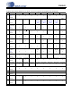
Figure 15. Left-Justified Format
LRCK
SCLK
MSB LSB
MSB
LSB
Left Channel Right Channel
SDIN
AOUTA
AOUTB
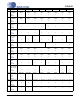
Figure 16. Right-Justified Format (DAC only)