
Instruction Manual

DS723F1 15
CS43L21
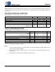
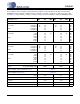
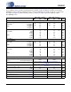
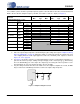
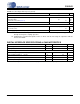
HEADPHONE OUTPUT POWER CHARACTERISTICS
Test conditions (unless otherwise specified): Input test signal is a full-scale 997 Hz sine wave; measurement band-
width is 10 Hz to 20 kHz; Sample Frequency = 48 kHz; test load R
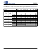
L
= 16 C
L
= 10 pF (see Figure 3).
4. One LSB of triangular PDF dither is added to data.
5. Full-scale output voltage and power is determined by the gain setting, G, in register “Headphone Analog
Gain (HP_GAIN[2:0])” on page 42. High gain settings at certain VA and VA_HP supply levels may
cause clipping when the audio signal approaches full-scale, maximum power output, as shown in
Figures 21 - 24 on page 56.
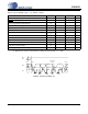
6. See Figure 3. R
L
and C
L
reflect the recommended minimum resistance and maximum capacitance re-
quired for the internal op-amp's stability and signal integrity. In this circuit topology, C
L
will effectively
move the band-limiting pole of the amp in the output stage. Increasing this value beyond the recom-
mended 150 pF can cause the internal op-amp to become unstable.
7. VA_HP settings lower than VA reduces the headroom of the headphone amplifier. As a result, the DAC
may not achieve the full THD+N performance at full-scale output voltage and power.
Parameter
VA = 2.5V (nominal)
Min Typ Max
VA = 1.8V (nominal)
Min Typ Max Unit
AOUTx Power Into R
L
= 16
HP_GAIN[2:0]
Analog
Gain (G)
VA_HP
000 0.3959
1.8 V - 14 - - 7 - mW
rms
2.5 V - 14 - - 7 - mW
rms
001 0.4571
1.8 V - 19 - - 10 - mW
rms
2.5 V - 19 - - 10 - mW
rms
010 0.5111
1.8 V - 23 - - 12 - mW
rms
2.5 V - 23 - - 12 - mW
rms
011 (default) 0.6047
1.8 V (Note 7) -17 -mW
rms
2.5 V - 32 - - 17 - mW
rms
100 0.7099
1.8 V (Note 7) -23 -mW
rms
2.5 V - 44 - - 23 - mW
rms
101 0.8399
1.8 V (Note 5) mW
rms
2.5 V -32 -mW
rms
110 1.0000
1.8 V
(Note 5, 7)
mW
rms
2.5 V mW
rms
111 1.1430
1.8 V mW
rms
2.5 V mW
rms
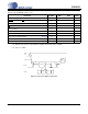
AOUTx
AGND
R
L
C
L
0.022 F
51
Figure 3. Headphone Output Test Load