
User Manual


DS568F1 7
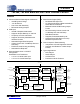
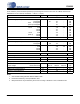
CS4398
Pin Name Pin # Pin Description
DSD_A
DSD_B
28
1
Direct Stream Digital Input (Input) - Input for Direct Stream Digital serial audio data.
DSD_SCLK 2 DSD Serial Clock (Input) - Serial clock for the Direct Stream Digital audio interface.
SDIN 3 Serial Audio Data Input (Input) - Input for two’s complement serial audio data.
SCLK 4 Serial Clock (Input) - Serial clock for the serial audio interface.
LRCK 5
Left Right Clock (Input) - Determines which channel, Left or Right, is currently active on
the serial audio data line.
MCLK 6 Master Clock (Input) - Clock source for the delta-sigma modulator and digital filters.
VD 7 Digital Power (Input) - Positive power for the digital section.
DGND 8 Digital Ground (Input) - Ground reference for the digital section.
RST 13 Reset
(Input) - The device enters system reset when enabled.
VLC 14 Control Port Power (Input) - Positive power for Control Port I/O.
FILT+ 15
Positive Voltage Reference (Output) - Positive reference voltage for the internal sam-
pling circuits.
REF_GND 16 Reference Ground (Input) - Ground reference for the internal sampling circuits.
VREF 17 Voltage Reference (Input) - Positive voltage reference for the internal sampling circuits.
BMUTEC
AMUTEC
18
25
Mute Control (Output) - The Mute Control pin is active during power-up initialization, mut-
ing, power-down or if the master clock to left/right clock frequency ratio is incorrect. During
reset, these outputs are set to a high impedance.
AOUTB+
AOUTB-
20
19
Differential Right Channel Analog Output (Output) - The full-scale differential analog
output level is specified in the Analog Characteristics specification table.
AGND 21 Analog Ground (Input) - Ground reference for the analog section.
VA 22 Analog Power (Input) - Positive power for the analog section.
AOUTA+
AOUTA-
23
24
Differential Left Channel Analog Output (Output) - The full-scale differential analog out-
put level is specified in the Analog Characteristics specification table.
VQ 26 Quiescent Voltage (Output) - Filter connection for internal quiescent voltage.
VLS 27 Serial Audio Interface Power (Input) - Positive power for serial audio interface I/O.
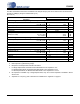
Stand-Alone Mode Definitions
M3
M2
M1
M0
9
10
11
12
Mode Selection (Input) - Determines the operational mode of the device.
Control Port Mode Definitions
AD1/CDIN 9
Address Bit 1 (I²C) / Control Data Input (SPI) (Input) - AD1 is a chip address pin in I²C
mode; CDIN is the input data line for the Control Port interface in SPI mode.
SCL/CCLK 10 Serial Control Port Clock (Input) - Serial clock for the serial Control Port.
SDA/CDOUT 11
Serial Control Data (I²C) / Control Data Output (SPI) (Input/Output) - SDA is a data I/O
line in I²C mode. CDOUT is the output data line for the Control Port interface in SPI mode.
AD0/CS
12
Address Bit 0 (I²C) / Control Port Chip Select (SPI) (Input) - AD0 is a chip address pin
in I²C mode; CS
is the chip select signal for SPI format.