
User Manual


DS568F1 29
CS4398
7. REGISTER DESCRIPTION
** All register access is R/W unless specified otherwise**
7.1 Chip ID - Register 01h
Function:
This register is Read-Only. Bits 7 through 3 are the part number ID, which is 01110b (14h), and the remain-
ing Bits (2 through 0) are for the chip revision (Rev. A = 000, Rev. B = 001, ...)
7.2 Mode Control 1 - Register 02h
7.2.1 DSD Input Source Select (DSD_SRC) BIT 7
Function:
When set to 0 (default), the dedicated DSD pins will be the active DSD inputs.
When set to 1, the source for DSD inputs will be as follows:
DSDA input on SDATA pin
DSDB input on LRCK pin
DSD_SCLK input on SCLK pin
The dedicated DSD pins must be tied low while not in use.
7.2.2 Digital Interface Format (DIF2:0) BITs 6-4
Function:
These bits select the interface format for the serial audio input. The Functional Mode bits determine
whether PCM or DSD mode is selected.
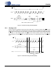
PCM Mode: The required relationship between the Left/Right clock, serial clock and serial data is defined
by the Digital Interface Format, and the options are detailed in Figures 3 through 5.
76543210
PART4 PART3 PART2 PART1 PART0 REV2 REV1 REV0
01110- - -
76543210
DSD_SRC DIF2 DIF1 DIF0 DEM1 DEM0 FM1 FM0
00000000
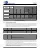
DIF2 DIF1 DIF0 Description Format Figure
000
Left-Justified, up to 24-bit data 0 (Default)
3
001
I²S, up to 24-bit data
14
010
Right-Justified, 16-bit data
25
011
Right-Justified, 24-bit data
35
100
Right-Justified, 20-bit data
45
101
Right-Justified, 18-bit data
55
110
Reserved
111
Reserved
Table 5. Digital Interface Formats - PCM Mode