CS4398 120 dB, 192 kHz Multi-Bit DAC with Volume Control Features Advanced Multi-bit Delta-Sigma Architecture – – – – Direct Stream Digital (DSD) 120 dB Dynamic Range -107 dB THD+N Low Clock Jitter Sensitivity Differential Analog Outputs – – – PCM input – – – – – – – – – 102 dB of Stopband Attenuation Supports Sample Rates up to 192 kHz Accepts up to 24 bit Audio Data Supports All Industry Standard Audio Interface Formats Selectable Digital Filter Response Volume Control with 1/2 dB Step Size
CS4398 Stand-Alone Mode Features Direct Stream Digital Mode Selectable Oversampling Modes Selectable Auto or Manual Mute Polarity – – – Selectable Interpolation Filters 32 kHz to 54 kHz Sampling Rates 50 kHz to 108 kHz Sampling Rates 100 kHz to 216 kHz Sampling Rates Selectable 32, 44.
CS4398 TABLE OF CONTENTS 1. PINOUT DRAWING ................................................................................................................. 6 2. CHARACTERISTICS AND SPECIFICATIONS ........................................................................ 8 SPECIFIED OPERATING CONDITIONS ................................................................................. 8 ABSOLUTE MAXIMUM RATINGS ...........................................................................................
CS4398 LIST OF FIGURES Figure 1. Pinout Drawing................................................................................................................. 6 Figure 2. Serial Mode Input Timing ............................................................................................... 12 Figure 3. Format 0 - Left-Justified up to 24-bit Data ..................................................................... 13 Figure 4. Format 1 - I²S up to 24-bit Data .............................................
CS4398 LIST OF TABLES Table 1. Clock Ratios .................................................................................................................... 21 Table 2. Common Clock Frequencies........................................................................................... 22 Table 3. Digital Interface Format, Stand-Alone Mode Options...................................................... 22 Table 4. Mode Selection, Stand-Alone Mode Options .....................................................
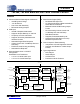
CS4398 1. PINOUT DRAWING DSD_B 1 28 DSD_A DSD_SCLK 2 27 VLS SDIN 3 26 VQ SCLK 4 25 AMUTEC LRCK 5 24 AOUTA- MCLK 6 23 AOUTA+ VD 7 22 VA DGND 8 21 AGND M3 (AD1/CDIN) 9 20 AOUTB+ M2 (SCL/CCLK) 10 19 AOUTB- M1 (SDA/CDOUT) 11 18 BMUTEC M0 (AD0/CS) 12 17 VREF RST 13 16 REF_GND VLC 14 15 FILT+ Figure 1.
CS4398 Pin Name Pin # Pin Description DSD_A DSD_B 28 1 Direct Stream Digital Input (Input) - Input for Direct Stream Digital serial audio data. DSD_SCLK 2 DSD Serial Clock (Input) - Serial clock for the Direct Stream Digital audio interface. SDIN 3 Serial Audio Data Input (Input) - Input for two’s complement serial audio data. SCLK 4 Serial Clock (Input) - Serial clock for the serial audio interface.
CS4398 2. CHARACTERISTICS AND SPECIFICATIONS (Min/Max performance characteristics and specifications are guaranteed over the Specified Operating Conditions. Typical performance characteristics are derived from measurements taken at TA = 25 °C, VA = 5.0 V, VD = 3.3 V.) SPECIFIED OPERATING CONDITIONS (AGND = 0 V; all voltages with respect to ground.
CS4398 ANALOG CHARACTERISTICS (Test conditions (unless otherwise specified): Input test signal is a 997 Hz sine wave at 0 dBFS; measurement bandwidth is 10 Hz to 20 kHz; test load RL = 1 kΩ, CL = 10 pF.) Parameter Symbol Min Typ Max Unit 114 111 - 120 117 97 94 - dB dB dB dB - -107 -97 -57 -94 -74 -34 -100 - dB dB dB dB dB dB - 120 - dB 111 108 117 114 - dB dB - -104 -94 -54 -98 - dB dB dB - 110 - dB - 0.
CS4398 COMBINED INTERPOLATION & ON-CHIP ANALOG FILTER RESPONSE The filter characteristics have been normalized to the sample rate (Fs) and can be referenced to the desired sample rate by multiplying the given characteristic by Fs.) (See note 9.) Fast Roll-Off Parameter Min Typ Max Combined Digital and On-Chip Analog Filter Response - Single-Speed Mode - 48 kHz (Note 5) Passband (Note 6) to -0.01 dB corner 0 .454 to -3 dB corner 0 .499 Frequency Response 10 Hz to 20 kHz -0.01 +0.01 StopBand 0.
CS4398 COMBINED INTERPOLATION & ON-CHIP ANALOG FILTER RESPONSE (Continued) Parameter Single-Speed Mode - 48 kHz (Note 5) Passband (Note 6) Frequency Response 10 Hz to 20 kHz StopBand StopBand Attenuation Group Delay De-emphasis Error (Note 8) (Relative to 1 kHz) Double-Speed Mode - 96 kHz (Note 5) Passband (Note 6) Frequency Response 10 Hz to 20 kHz StopBand StopBand Attenuation Group Delay Quad-Speed Mode - 192 kHz (Note 5) Passband (Note 6) Frequency Response 10 Hz to 20 kHz StopBand StopBand Attenuation
CS4398 SWITCHING CHARACTERISTICS (Inputs: Logic 0 = GND, Logic 1 = VLS, CL = 20 pF) Parameters Input Sample Rate Single-Speed Mode Double-Speed Mode Quad-Speed Mode MCLK Frequency Symbol Min Typ Max Units Fs Fs Fs 30 50 100 - 54 108 216 kHz kHz kHz See Tables 1 & 2 (page 21) for compatible frequencies MCLK Duty Cycle 40% - 60% LRCK Duty Cycle 45% 50 55% SCLK Pulse Width Low tsclkl 20 - - ns SCLK Pulse Width High tsclkh 20 - - ns tsclkw 1 --------------------( 128 )Fs - -
CS4398 Left C ha nnel LR C K R ig h t C ha n nel SCLK SDATA M SB -1 -2 -3 -4 -5 +5 +4 +3 +2 +1 LSB M SB -1 -2 -3 -4 +5 +4 +3 +2 +1 LSB Figure 3. Format 0 - Left-Justified up to 24-bit Data Left C ha nnel LR C K R ig h t C ha n nel SCLK SDATA MSB -1 -2 -3 -4 -5 +5 +4 +3 +2 +1 LSB MSB -1 -2 -3 -4 +5 +4 +3 +2 +1 LSB Figure 4.
CS4398 SWITCHING CHARACTERISTICS - DSD (Logic 0 = AGND = DGND; Logic 1 = VLS Volts; CL = 20 pF) Parameter MCLK Duty Cycle DSD_SCLK Pulse Width Low DSD_SCLK Pulse Width High DSD_SCLK Frequency Symbol Min 40 160 160 1.024 2.048 20 20 -20 tsclkl tsclkh (64x Oversampled) (128x Oversampled) DSD_A / _B valid to DSD_SCLK rising setup time DSD_SCLK rising to DSD_A or DSD_B hold time DSD clock to data transition (Phase Modulation mode) tsdlrs tsdh tdpm t t Typ - Max 60 3.2 6.
CS4398 SWITCHING CHARACTERISTICS - CONTROL PORT - I²C FORMAT (Inputs: Logic 0 = GND, Logic 1 = VLC, CL = 20 pF) Parameter Symbol Min Max Unit fscl - 100 kHz RST Rising Edge to Start tirs 500 - ns Bus Free-Time Between Transmissions tbuf 4.7 - µs Start Condition Hold Time (prior to first clock pulse) thdst 4.0 - µs Clock Low Time tlow 4.7 - µs Clock High Time thigh 4.0 - µs Setup Time for Repeated Start Condition tsust 4.
CS4398 SWITCHING CHARACTERISTICS - CONTROL PORT - SPI™ FORMAT (Inputs: Logic 0 = GND, Logic 1 = VLC, CL = 20 pF) Parameter Symbol Min Max Unit CCLK Clock Frequency fsclk - 6 MHz RST Rising Edge to CS Falling tsrs 500 - ns tspi 500 - ns CS High Time Between Transmissions tcsh 1.
CS4398 DC ELECTRICAL CHARACTERISTICS Parameters Normal Operation (Note 16) Power Supply Current Min Typ Max Units IA Iref ID ID ILC ILS - 25 1.5 25 18 2 80 28 2 38 27 - mA mA mA mA µA µA - 258 192 340 240 mW mW Ipd - 200 1 1 - µA mW mW PSRR - 60 40 0.5•VA 1 0.93•VA 3 VA 0 - dB dB V µA V mA V V VA= 5 V (Note 17) Vref= 5 V VD = 5 V VD = 3.
CS4398 DIGITAL INTERFACE SPECIFICATIONS Parameters High-Level Output Voltage (IOH = -1.2 mA) Serial I/O Control I/O Serial I/O Control I/O Control I/O VIH VIH VIL VIL VOH Min 70% 70% 80% Low-Level Output Voltage (IOL = 1.
CS4398 3. TYPICAL CONNECTION DIAGRAM +3.3V to +5V 10 uF +5V 0.1 uF 10 uF 0.1 uF VD VA System Clock MCLK PCM Digital Audio Source AMUTEC SCLK AOUTA - LRCK AOUTA+ SDIN +1.8V to 0.1 uF +5V Left Channel Analog Conditioning and Mute VLS AOUTB+ DSD_SCLK DSD Audio Source DSD_A AOUTB - DSD_B Right Channel Analog Conditioning and Mute BMUTEC CS4398 +1.8V to 0.1 uF +5V VLC VQ M0 (AD0/CS) µControler or stand alone pull-ups/ downs 3.3 uF FILT+ M1 (SDA/CDOUT) 0.1 uF 100 uF 0.
CS4398 4. APPLICATIONS 4.1 Grounding and Power Supply Decoupling As with any high resolution converter, the CS4398 requires careful attention to power supply and grounding arrangements to optimize performance. The Typical Connection Diagram shows the recommended power arrangement with VA, VD, VLS and VLC connected to clean supplies. Decoupling capacitors should be located as close to the device package as possible.
CS4398 Use of the Mute Control function is not mandatory but recommended for designs requiring the absolute minimum in extraneous clicks and pops. Also, use of the Mute Control function can enable the system designer to achieve idle channel noise/signal-to-noise ratios which are only limited by the external mute circuit. Figure 12. Recommended Mute Circuitry 4.4 Oversampling Modes The CS4398 operates in one of three oversampling modes based on the input sample rate.
CS4398 MCLK (MHz) Sample Mode Rate (sampleMCLKDIV2 MCLKDIV3 (kHz) rate range) MCLK Ratio 256x 384x 512x 768x 1024x 1152x 32 8.1920 12.2880 16.3840 24.5760 32.7680 36.8640 Single-Speed (32 to 50 kHz) 44.1 11.2896 16.9344 22.5792 33.8688 45.1584 48 12.2880 18.4320 24.5760 36.8640 49.1520 MCLK Ratio 128x 192x 256x 384x 512x 64 8.1920 12.2880 16.3840 24.5760 32.7680 Double-Speed (50 to 100 kHz) 88.2 11.2896 16.9344 22.5792 33.8688 45.1584 96 12.2880 18.4320 24.5760 36.8640 49.
CS4398 4.6.1 Recommended Power-up Sequence (Stand-Alone Mode) 1. Hold RST low until the power supply, master, and left/right clocks are stable. In this state, the Control Port is reset to its default settings. 2. Bring RST high. The device will remain in a low power state and will initiate the Stand-Alone powerup sequence following approximately 218 MCLK cycles. 4.7 Control Port Mode 4.7.1 Recommended Power-up Sequence (Control Port Mode) 1.
CS4398 4.7.6 Direct Stream Digital (DSD) Mode (Control Port Mode) In Control Port mode, the FM bits (Reg. 02h) are used to configure the device for DSD mode. The DIF bits (Reg 02h) then control the expected DSD rate and MCLK ratio. The DSD_SRC bit (Reg. 02h) selects the input pins for DSD clocks and data. During DSD operation, the PCM-related pins should either be tied low or remain active with clocks.
CS4398 5. CONTROL PORT INTERFACE The Control Port is used to load all the internal settings. The operation of the Control Port may be completely asynchronous with the audio sample rate. However, to avoid potential interference problems, the Control Port pins should remain static if no operation is required. 5.1 Memory Address Pointer (MAP) 5.1.1 Memory Address Pointer (MAP) Register Detail 7 INCR 0 6 Reserved 0 5.1.
CS4398 5.4.1 Writing in I²C Format To communicate with the CS4398, initiate a START condition of the bus (see Figure 14.). Next, send the chip address. The eighth bit of the address byte is the R/W bit (low for a write). The next byte is the Memory Address Pointer, MAP, which selects the register to be read or written. The MAP is then followed by the data to be written. To write multiple registers, continue providing a clock and data, waiting for the CS4398 to acknowledge between each byte.
CS4398 CS CCLK CHIP MAP ADDRESS CDIN 1001100 DATA LSB MSB R/W byte 1 byte n MAP = Memory Address Pointer Figure 15. Control Port Timing, SPI Format (Write) 5.5.2 Reading in SPI Figure 16 shows the operation of the Control Port in SPI format. To read to a register, bring CS low. The first seven bits on CDIN form the chip address and must be 1001100. The eighth bit is a read/write control (R/W), which must be high to read.
CS4398 6. Addr REGISTER QUICK REFERENCE Function 1h Chip ID default 2h Mode Control default 3h Volume, Mixing, and Inversion Control default 4h Mute Control default 5h Channel A Volume Control default 6h Channel B Volume Control default 7h Ramp and Filter Control default 8h Misc. Control default 9h Misc.
CS4398 7. REGISTER DESCRIPTION ** All register access is R/W unless specified otherwise** 7.1 Chip ID - Register 01h 7 PART4 6 PART3 5 PART2 4 PART1 3 PART0 2 REV2 1 REV1 0 REV0 0 1 1 1 0 - - - Function: This register is Read-Only. Bits 7 through 3 are the part number ID, which is 01110b (14h), and the remaining Bits (2 through 0) are for the chip revision (Rev. A = 000, Rev. B = 001, ...) 7.
CS4398 DSD Mode: The relationship between the oversampling ratio of the DSD audio data and the required Master Clock to DSD data rate is defined by the Digital Interface Format pins.
CS4398 7.3.1 Channel B Volume = Channel A Volume (VOLB=A) Bit 7 Function: When set to 0 (default), the AOUTA and AOUTB volume levels are independently controlled by the A and the B Channel Volume Control Bytes. When set to 1, the volume on both AOUTA and AOUTB are determined by the A Channel Attenuation and Volume Control Bytes, and the B Channel Bytes are ignored. 7.3.2 Invert Signal Polarity (Invert_A) Bit 6 Function: When set to 1, this bit inverts the signal polarity of channel A.
CS4398 32 ATAPI4 ATAPI3 ATAPI2 ATAPI1 ATAPI0 AOUTA AOUTB 0 0 0 0 0 MUTE MUTE 0 0 0 0 1 MUTE bR 0 0 0 1 0 MUTE bL 0 0 0 1 1 MUTE b[(L+R)/2] 0 0 1 0 0 aR MUTE 0 0 1 0 1 aR bR 0 0 1 1 0 aR bL 0 0 1 1 1 aR b[(L+R)/2] 0 1 0 0 0 aL MUTE 0 1 0 0 1 aL bR 0 1 0 1 0 aL bL 0 1 0 1 1 aL b[(L+R)/2] 0 1 1 0 0 a[(L+R)/2] MUTE 0 1 1 0 1 a[(L+R)/2] bR 0 1 1 1 0 a[(L+R)/2] bL 0 1 1 1 1 a[(L+R)/2] b[(L+R)/2]
CS4398 7.4 Mute Control - Register 04h 7 6 5 4 3 2 1 0 PAMUTE 1 DAMUTE 1 MUTEC A=B 0 MUTE_A 0 MUTE_B 0 Reserved 0 MUTEP1 0 MUTEP0 0 7.4.1 PCM Auto-mute (PAMUTE) Bit 7 Function: When set to 1 (default), the Digital-to-Analog converter output will mute following the reception of 8192 consecutive audio samples of static 0 or -1. A single sample of non-static data will release the mute. Detection and muting is done independently for each channel.
CS4398 7.4.5 MUTE Polarity and DETECT (MUTEP1:0) Bits 1-0 Default = 00 00 - Auto polarity detect, selected from AMUTEC pin 01 - Reserved 10 - Active low mute polarity 11 - Active high mute polarity Function: Auto mute polarity detect (00) See section 4.3 on page 20 for description. Active low mute polarity (10) When RST is low, the outputs are high-impedance and will need to be biased active. Once reset has been released and after this bit is set, the MUTEC output pins will be active low polarity.
CS4398 7.7 Ramp and Filter Control - Register 07h 7 6 5 4 3 2 1 0 SZC1 1 SZC0 0 RMP_UP 1 RMP_DN 1 Reserved 0 FILT_SEL 0 Reserved 0 DIR_DSD 0 7.7.
CS4398 7.7.2 Soft Volume Ramp-up after Error (RMP_UP) Bit 5 Function: An un-mute will be performed after executing an LRCK/MCLK ratio change or error, and after changing the Functional Mode. When set to 1 (default), this un-mute is effected, similar to attenuation changes, by the Soft and Zero Cross bits in the Volume and Mixing Control register. When set to 0, an immediate un-mute is performed in these instances. Notes: 7.7.
CS4398 7.8 Misc. Control - Register 08h 7 6 5 4 3 2 1 0 PDN 1 CPEN 0 FREEZE 0 MCLKDIV2 0 MCLKDIV3 0 Reserved 0 Reserved 0 Reserved 0 7.8.1 Power Down (PDN) Bit 7 Function: When set to 1 (default), the entire device enters a low-power state, and the contents of the control registers is retained. The power-down bit defaults to ‘1’ on power-up and must be disabled before normal operation in Control Port mode can occur. This bit is ignored if CPEN is not set. 7.8.
CS4398 7.9 Misc. Control - Register 09h 7 6 5 4 3 2 Reserved Reserved Reserved Reserved STATIC_DSD INVALID_DSD 0 0 0 0 1 0 7.9.1 1 0 DSD_PM_MODE 0 DSD_PM_EN 0 Static DSD Detect (Static_DSD) Bit 3 Function: When set to 1 (default), the DSD processor checks for 28 consecutive zeroes or ones and, if detected, sends a mute signal to the DACs. The MUTEC pins will eventually go active according to the DAMUTE register. When set to 0, this function is disabled. 7.9.
CS4398 8. PARAMETER DEFINITIONS Total Harmonic Distortion + Noise (THD+N) THD+N is the ratio of the rms value of the signal to the rms sum of all other spectral components over the specified bandwidth (typically 10 Hz to 20 kHz), including distortion components. Expressed in decibels. Dynamic Range The ratio of the full-scale rms value of the signal to the rms sum of all other spectral components over the specified bandwidth.
CS4398 10.PACKAGE DIMENSIONS 10.1 28-TSSOP N D E11 A2 E e b2 A ∝ A1 SIDE VIEW L END VIEW SEATING PLANE 1 2 3 TOP VIEW DIM A A1 A2 b D E E1 e L µ MIN -0.002 0.03150 0.00748 0.378 BSC 0.248 0.169 -0.020 0° Inches NOM -0.004 0.035 0.0096 0.382 BSC 0.2519 0.1732 0.026 BSC 0.024 4° MAX 0.47 0.006 0.04 0.012 0.386 BSC 0.256 0.177 -0.029 8° MIN -0.05 0.80 0.19 9.60 BSC 6.30 4.30 -0.50 0° Millimeters NOM -0.10 0.90 0.245 9.70 BSC 6.40 4.40 0.65 BSC 0.60 4° Note MAX 1.20 0.15 1.00 0.30 9.
CS4398 0 0 −20 −20 −40 −40 Amplitude (dB) Amplitude (dB) 11.APPENDIX −60 −60 −80 −80 −100 −100 −120 0.4 0.5 0.6 0.7 0.8 Frequency(normalized to Fs) 0.9 −120 0.4 1 Figure 20. Single-Speed (fast) Stopband Rejection 0.42 0.44 0.46 0.48 0.5 0.52 Frequency(normalized to Fs) 0.54 0.56 0.58 0.6 Figure 21. Single-Speed (fast) Transition Band 0.02 0 −1 0.015 −2 0.01 0.005 −4 Amplitude (dB) Amplitude (dB) −3 −5 −6 0 −0.005 −7 −0.01 −8 −0.015 −9 −10 0.45 0.46 0.47 0.
CS4398 0.02 0 −1 0.015 −2 0.01 0.005 −4 Amplitude (dB) Amplitude (dB) −3 −5 −6 0 −0.005 −7 −0.01 −8 −0.015 −9 −10 0.45 0.46 0.47 0.48 0.49 0.5 0.51 Frequency(normalized to Fs) 0.52 0.53 0.54 −0.02 0.55 Figure 26. Single-Speed (slow) Transition Band (detail) 0.1 0.15 0.2 0.25 0.3 Frequency(normalized to Fs) 0.35 0.4 0.45 0.5 0 20 20 40 40 Amplitude (dB) Amplitude (dB) 0.05 Figure 27. Single-Speed (slow) Passband Ripple 0 60 60 80 80 100 100 120 0 120 0.
CS4398 0 20 20 40 40 Amplitude (dB) Amplitude (dB) 0 60 60 80 80 100 100 120 120 0.2 0.3 0.4 0.5 0.6 0.7 Frequency(normalized to Fs) 0.8 0.9 1 Figure 32. Double-Speed (slow) Stopband Rejection 0.2 0.3 0.4 0.5 0.6 Frequency(normalized to Fs) 0.7 0.8 Figure 33. Double-Speed (slow) Transition Band 0 0.02 1 0.015 2 0.01 0.005 4 Amplitude (dB) Amplitude (dB) 3 5 6 0 0.005 7 0.01 8 0.015 9 10 0.45 0.46 0.47 0.48 0.49 0.5 0.51 Frequency(normalized to Fs) 0.52 0.
CS4398 0.2 0 1 0.15 2 0.1 3 Amplitude (dB) Amplitude (dB) 0.05 4 5 6 0 0.05 7 0.1 8 0.15 9 10 0.45 0.2 0.46 0.47 0.48 0.49 0.5 0.51 Frequency(normalized to Fs) 0.52 0.53 0.54 0.55 0 Figure 38. Quad-Speed (fast) Transition Band (detail) 0.05 0.1 0.15 Frequency(normalized to Fs) 0.2 0.25 Figure 39. Quad-Speed (fast) Passband Ripple 0 0 20 40 40 Amplitude (dB) Amplitude (dB) 20 60 60 80 80 100 100 120 120 0.1 0.2 0.3 0.4 0.5 0.6 0.
CS4398 Release A1 Date Changes November 2002 Initial Release PP1 July 2003 -Updated Legal Notice on page 46. -Moved Min/Max/Typ spec note from “ANALOG CHARACTERISTICS” (on page 9) to “CHARACTERISTICS AND SPECIFICATIONS” on page 8. -Changed heading “RECOMMENDED OPERATING CONDITIONS” to “SPECIFIED OPERATING CONDITIONS” on page 8.
CS4398 Contacting Cirrus Logic Support For all product questions and inquiries contact a Cirrus Logic Sales Representative. To find one nearest you go to www.cirrus.com IMPORTANT NOTICE Cirrus Logic, Inc. and its subsidiaries ("Cirrus") believe that the information contained in this document is accurate and reliable. However, the information is subject to change without notice and is provided "AS IS" without warranty of any kind (express or implied).