
Manual

CS4397
DS333F1 23
5.0 PIN DESCRIPTION - DSD MODE
Master Clock - MCLK
Pin 10, Input
Function:
The master clock frequency must be either 4x or 6x the DSD data rate for 64x oversampled DSD data
and 2x or 3x the DSD data rate for 128x oversampled DSD data, refer to Table 7.
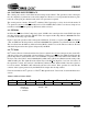
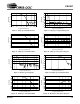
CLKMODE
Pin 12, Input
Function:
This pin determines the allowable Master Clock to DSD data ratio as defined in Table 7.
DSD Serial Clock - DSD_SCLK
Pin 11, Input
Function:
Clocks the individual bits of the DSD audio data into the DSD_L and DSD_R pins.
Audio Data - DSD_L and DSD_R
Pins 13 and 14, Inputs
Function:
Direct Stream Digital audio data is clocked into DSD_L and DSD_R via the DSD serial clock.
CLKMODE
DSD Over-
Sampling Ratio
01
64x 4x 6x
128x 2x 3x
Table 7. MCLK to DSD Data Rate Clock Ratios
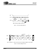
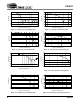
Refer to PCM mode RST VREF Refer to PCM mode
Refer to PCM mode M4(ADO/CS
) FILT+ Refer to PCM mode
Refer to PCM mode M3(AD1/CDIN) FILT- Refer to PCM mode
Refer to PCM mode M2(SCL/CCLK) CMOUT Refer to PCM mode
Refer to PCM mode M0(SDA/CDOUT) AOUTL- Refer to PCM mode
Refer to PCM mode DGND AOUTL+ Refer to PCM mode
Refer to PCM mode VD VA Refer to PCM mode
Refer to PCM mode VD AGND Refer to PCM mode
Refer to PCM mode DGND AOUTR+ Refer to PCM mode
Master Clock MCLK AOUTR- Refer to PCM mode
DSD Serial Clock DSD_SCLK AGND Refer to PCM mode
Master Clock Mode CLKMODE MUTEC
Refer to PCM mode
Left Channel Data DSD_L C/H
Refer to PCM mode
Right Channel Data DSD_R MUTE
Refer to PCM mode
1
2
3
4
5
6
7
8
9
10
11
12
5
1
2
6
28
27
26
25
24
23
22
21
20
19
18
17
13
14
16
15