CS4396 24-Bit, 192 kHz D/A Converter for Digital Audio Features Description l 24 The CS4396 is a complete high performance 24-bit 48/96/192 kHz stereo digital-to-analog conversion system. The device includes a digital interpolation filter followed by a oversampled multi-bit delta-sigma modulator which drives dynamic-element-matching (DEM) selection logic. The output from the DEM block controls the input to a multi-element switched capacitor DAC/lowpass filter, with fully-differential outputs.
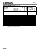
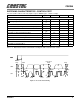
CS4396 TABLE OF CONTENTS 1.0 CHARACTERISTICS/SPECIFICATIONS ..................................................................... 4 ANALOG CHARACTERISTICS................................................................................... 4 Dynamic Performance - Single Speed Mode - Fs equal to 48 kHz ...................... 4 Dynamic Performance - Double Speed Mode - Fs equal to 96 kHz .................... 4 Dynamic Performance - Quad-Speed Mode - Fs equal to 192 kHz .....................
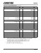
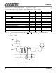
CS4396 TABLE OF FIGURES Figure 1. Serial Audio Input Timing ........................................................................... 8 Figure 2. I2C Control Port Timing .............................................................................. 9 Figure 3. SPI Control Port Timing ........................................................................... 10 Figure 4. Typical Connection Diagram - Hardware Mode (Control Port Mode) ....... 11 Figure 5. Control Port Timing, I2C Mode ......................
CS4396 1.0 CHARACTERISTICS/SPECIFICATIONS ANALOG CHARACTERISTICS (TA = 25 °C; Logic "1" = VD = 5 V; VA = 5V; Logic "0" = DGND; Full-Scale Output Sine Wave, 997 Hz; MCLK = 12.288 MHz; SCLK = 3.072 MHz, Measurement Bandwidth 10 Hz to 20 kHz, unless otherwise specified.
CS4396 ANALOG CHARACTERISTICS (Continued) Parameter Power Supplies Supply Current VA = 5 V Symbol normal operation normal operation power-down state Power Dissipation VA = 5 V IA ID ID + IA normal operation power-down Power Supply Rejection Ratio (1 kHz) (Note 3) (120 Hz) Parameter Analog Output Full Scale Differential Output Voltage Common Mode Voltage Interchannel Gain Mismatch Gain Drift Differential DC Offset AC-Load Resistance Load Capacitance Interchannel Isolation PSRR Symbol RL CL (1 kHz
CS4396 ANALOG CHARACTERISTICS Parameter (Continued) Symbol Min Typ Combined Digital and On-chip Analog Filter Response - Single Speed Mode Passband (Note 4) to -0.1 dB corner to -3 dB corner Frequency Response 10 Hz to 20 kHz -.020 Passband Ripple StopBand .5465 StopBand Attenuation (Note 5) 102 Group Delay (Note 6) tgd 37/Fs De-emphasis Error (Note 7) Fs = 32 kHz (Relative to 1 kHz) Fs = 44.
CS4396 DIGITAL CHARACTERISTICS (TA = 25°C; VD = 3.0V - 5.25V) Parameters High-Level Input Voltage Low-Level Input Voltage Input Leakage Current Input Capacitance Maximum MUTEC Drive Current VD = 5 V VD = 3 V VD = 5 V VD = 3 V Symbol VIH VIL Iin Min 2.0 2.0 - Typ 8 3 Max 0.8 0.8 ±10 - Units V V V V µA pF mA ABSOLUTE MAXIMUM RATINGS (AGND = 0 V, all voltages with respect to ground.
CS4396 SWITCHING CHARACTERISTICS (TA= -10 to 70°C; Logic 0 = AGND = DGND; Logic 1 = VD = 5.25 to 3.
CS4396 SWITCHING CHARACTERISTICS - CONTROL PORT (TA = 25 °C; VD = 5.25 V to 3.0 Volts; Inputs: logic 0 = AGND, logic 1 = VD, CL = 30 pF) Parameter Symbol Min Max Unit Mode SCL Clock Frequency fscl - 100 KHz RST Rising Edge to Start tirs 500 - ns Bus Free Time Between Transmissions tbuf 4.7 - µs Start Condition Hold Time (prior to first clock pulse) thdst 4.0 - µs Clock Low time tlow 4.7 - µs Clock High Time thigh 4.0 - µs Setup Time for Repeated Start Condition tsust 4.
CS4396 SWITCHING CHARACTERISTICS - CONTROL PORT (TA = 25 °C; VD = 5.25 V to 3.0 Volts; Inputs: logic 0 = AGND, logic 1 = VD, CL = 30 pF) Parameter Symbol Min Max Unit SPI Mode CCLK Clock Frequency fsclk - 6 MHz RST Rising Edge to CS Falling tsrs 500 - ns tspi 500 - ns CS High Time Between Transmissions tcsh 1.
CS4396 2.0 TYPICAL CONNECTION DIAGRAM + 1 µF 0.1 µF 5 Mode Select 14 4 3 2 0.1 µf +1.0 µ F 7 VD M0 8 22 VA VREF M1 CS4396 M2 +5V Analog 28 FILT+ 27 0.1 µf + 10 µf FILT- 26 M3 M4 AOUTL12 +5V Analog 24 Analog Conditioning LRCK AOUTL+ 23 11 Audio Data Processor 13 SCLK MUTEC 17 SDATA AOUTR15 1 19 Analog Conditioning MUTE RST 10 MCLK 16 C/H DGND 9 6 AOUTR+ 20 CMOUT 25 AGND 18 21 0.1 µf + 10 µf External Clock Figure 4.
CS4396 3.0 REGISTER DESCRIPTION 3.1 DIFFERENTIAL DC OFFSET CALIBRATION Mode Control Register (address 01h) 7 CAL 6 MUTE 5 M4 4 M3 3 M2 2 M1 1 M0 0 PDN Access: R/W in I2C and SPI. Default: 0 - Disabled Function: Enabling this function will initiate a calibration to minimize the differential DC offset. This function will be automatically reset following completion of the calibration sequence. CAL 0 1 MODE Disabled : CAL complete Enabled : CAL initiated Table 1. 3.
CS4396 3.3 MODE SELECT Mode Control Register (address 01h) 7 CAL 6 MUTE 5 M4 4 M3 3 M2 2 M1 1 M0 0 PDN Access: R/W in I2C and SPI. Default: 00000 Function: The Mode Select pins determine the operational mode of the device as detailed in Tables 7-10.
CS4396 4.
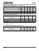
CS4396 Sample Rate (kHz) 32 44.1 48 256x 8.1920 11.2896 12.2880 MCLK (MHz) 384x 512x 12.2880 16.3840 16.9344 22.5792 18.4320 24.5760 768x 24.5760 33.8688 36.8640 Table 4. Single Speed (16 to 50 kHz sample rates) Common Clock Frequencies Sample Rate (kHz) 64 88.2 96 128x 8.1920 11.2896 12.2880 MCLK (MHz) 192x 256x 12.2880 16.3840 16.9344 22.5792 18.4320 24.5760 384x 24.5760 33.8688 36.8640 Table 5. Double Speed (50 to 100 kHz sample rates) Common Clock Frequencies Sample Rate (kHz) 176.
CS4396 cles in Single Speed, 2304 cycles in Double Speed and 4608 cycles in Quad Speed mode. The bias voltage on the outputs will be retained and MUTEC will go active at the completion of the ramp period. The analog outputs will ramp to a normal state when this function transitions from the enabled to disabled state. The ramp requires 1152 left/right clock cycles in Single Speed, 2304 cycles in Double Speed and 4608 cycles in Quad Speed mode. The MUTEC will release immediately on setting MUTE = 1.
CS4396 Common Mode Voltage - CMOUT Pin 25, Output Function: Filter connection for internal bias voltage, typically 50% of VREF. Capacitors must be connected from CMOUT to analog ground, as shown in Figure 4. CMOUT has a typical source impedence of 25 kΩ and any current drawn from this pin will alter device performance Reference Ground - FILT- Pin 26, Input Function: Ground reference for the internal sampling circuits. Must be connected to analog ground.
CS4396 Address Bit 1 / Control Data Input - AD1/CDIN Pin 3, Input Function: In I2C mode, AD1 is a chip address bit. CDIN is the control data input line for the control port interface in SPI mode. Serial Control Interface Clock - SCL/CCLK Pin 4, Input Function: In I2C mode, SCL clocks the serial control data into or from SDA/CDOUT. In SPI mode, CCLK clocks the serial data into AD1/CDIN and out of SDA/CDOUT.
CS4396 5.0 APPLICATIONS 5.1 Recommended Power-up Sequence 1. Hold RST low until the power supplies, master, and left/right clocks are stable. 2. Bring RST high.
CS4396 6.0 CONTROL PORT INTERFACE The control port is used to load all the internal settings of the CS4396. The operation of the control port may be completely asynchronous to the audio sample rate. However, to avoid potential interference problems, the control port pins should remain static if no operation is required. The control port has 2 modes: SPI and I2C, with the CS4396 operating as a slave device in both modes. If I2C operation is desired, AD0/CS should be tied to VD or DGND.
CS4396 CS CCLK CHIP ADDRESS CDIN MAP 0010000 R/W DATA LSB MSB byte 1 byte n MAP = Memory Address Pointer = 0 Figure 5. Control Port Timing, SPI mode Note 1 SDA 001000 ADDR AD0 R/W ACK DATA 1-8 ACK DATA 1-8 ACK SCL Start Stop Note: If operation is a write, this byte contains the Memory Address Pointer, MAP. Figure 6.
CS4396 M4 0 0 0 0 M1 (DIF1) 0 0 1 1 M0 (DIF0) 0 1 0 1 DESCRIPTION FORMAT FIGURE 0 1 2 3 20 21 22 23 Left Justified, up to 24-bit data I2S, up to 24-bit data Right Justified, 16-bit Data Right Justified, 24-bit Data Table 7. Single Speed (16 to 50 kHz) Digital Interface Format Options M4 0 0 0 0 M3 (DEM1) 0 0 1 1 M2 (DEM0) 0 1 0 1 DESCRIPTION 32 kHz De-Emphasis 44.1 kHz De-Emphasis 48 kHz De-Emphasis De-Emphasis Disabled FIGURE 19 19 19 - Table 8.
0 0 -20 -20 -40 -40 Amplitude dB Amplitude dB CS4396 -60 -80 -100 -60 -80 -100 -120 -120 -140 -140 -160 0.460.47 0.48 0.480.49 0.50.50 0.56 0.580.59 0.6 0.6 0.45 0.46 0.51 0.520.52 0.53 0.540.54 0.55 0.56 0.57 0.58 -160 0.45 0.5 0.55 0.6 0 0.1 -1 0.08 -2 0.06 -3 0.04 -4 -5 -6 -7 0.8 0.85 0.9 0.95 1 0 -0.02 -0.04 -8 -0.06 -9 -0.08 -0.1 0.46 0.47 0.48 0.49 0.5 0.51 0.52 0 0.05 0.1 0.15 0.2 0.25 0.3 0.35 0.4 0.45 Frequency (normalized to Fs) Figure 9.
0 0 -20 -20 -40 -40 Amplitude dB Amplitude dB CS4396 -60 -80 -100 -60 -80 -100 -120 -120 -140 -140 -160 -160 0.4 0.45 0.5 0.55 0.6 0.65 0.7 0.75 0.8 0.85 0.9 0.95 1 0.5 0.52 0.54 0.56 Frequency (normalized to Fs) 0.6 0.62 0.64 0.66 0.68 0.7 Figure 16. Quad-speed Transition Band 0 0.1 -1 0.08 -2 0.06 -3 0.04 Amplitude dB Amplitude dB Figure 15. Quad-speed Stopband Rejection -4 -5 -6 -7 0.02 0 -0.02 -0.04 -8 -0.06 -9 -0.08 -10 0.35 0.
CS4396 Left Channel LRCK Right Channel SCLK SDATA MSB -1 -2 -3 -4 -5 +5 +4 +3 +2 +1 LSB +5 +4 +3 +2 +1 LSB MSB -1 -2 -3 -4 Figure 20. Format 0, Left Justified Left Channel LRCK Right Channel SCLK SDATA MSB -1 -2 -3 -4 -5 +5 +4 +3 +2 +1 LSB MSB -1 -2 -3 -4 +5 +4 +3 +2 +1 LSB Figure 21. Format 1, I2S LRCK Right Channel Left Channel SCLK SDATA 15 14 13 12 11 10 9 8 7 6 5 4 3 2 1 0 15 14 13 12 11 10 9 8 7 6 5 4 3 2 1 0 32 clocks Figure 22.
CS4396 7.0 PARAMETER DEFINITIONS Total Harmonic Distortion + Noise (THD+N) The ratio of the rms value of the signal to the rms sum of all other spectral components over the specified bandwidth (typically 10Hz to 20kHz), including distortion components. Expressed in decibels. Dynamic Range The ratio of the full scale rms value of the signal to the rms sum of all other spectral components over the specified bandwidth.
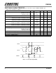
CS4396 9.0 PACKAGE DIMENSIONS 28L SOIC (300 MIL BODY) PACKAGE DRAWING E H 1 b c ∝ D L SEATING PLANE A e A1 DIM A A1 B C D E e H L ∝ INCHES MIN 0.093 0.004 0.013 0.009 0.697 0.29G10 1 0.040 0.394 0.016 0° MAX 0.104 0.012 0.020 0.013 0.713 0.299 MILLIMETERS MIN MAX 2.35 2.65 0.10 0.30 0.33 0.51 0.23 0.32 17.70 18.10 7.40 7.60 0.060 0.419 0.050 8° 1.02 10.00 0.40 0° 1.52 10.65 1.