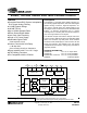
CS4392 24-Bit, 192 kHz Stereo DAC with Volume Control Features Description z Complete Stereo DAC System: Interpolation, The CS4392 is a complete stereo digital-to-analog system including digital interpolation, fifth-order delta-sigma digital-to-analog conversion, digital de-emphasis, volume control, channel mixing and analog filtering.
CS4392 TABLE OF CONTENTS 1. PIN DESCRIPTION - PCM DATA MODE .................................................................... 5 1.1 PIN DESCRIPTION - DSD mode ..................................................................... 6 2. TYPICAL CONNECTION DIAGRAMS ........................................................................ 7 3. APPLICATIONS ........................................................................................................... 9 3.
CS4392 6.2.2 Soft Ramp or Zero Cross Enable (Bits 6:5) ...........................................20 6.2.3 ATAPI Channel Mixing and Muting (Bits 4:0) .........................................20 6.3 Channel A Volume Control - Address 03h ......................................................22 6.4.1 Mute (Bit 7) ............................................................................................22 6.4.2 Volume Control (Bits 6:0) .......................................................................
CS4392 LIST OF FIGURES Figure 1. Typical Connection Diagram - PCM Mode....................................................................... 7 Figure 2. Typical Connection Diagram - DSD Mode ....................................................................... 8 Figure 3. CS4392 Output Filter ....................................................................................................... 9 Figure 4. Format 0, Left Justified up to 24-Bit Data.........................................................
CS4392 1. PIN DESCRIPTION - PCM DATA MODE RST VL SDATA SCLK LRCK MCLK M3 (SCL/CCLK) M2 (SDA/CDIN) M1 (AD0/CS) M0 1 2 3 4 5 6 7 8 9 10 20 19 18 17 16 15 14 13 12 11 AMUTEC AOUTAAOUTA+ VA AGND AOUTB+ AOUTBBMUTEC CMOUT FILT+ RST 1 Reset (Input) - Powers down device and resets all internal registers to their default settings. VL 2 Logic Power (Input) - Positive power for the digital input/output. SDATA 3 Serial Audio Data (Input) - Input for two’s complement serial audio data.
CS4392 1.1 PIN DESCRIPTION - DSD mode RST VL DSD_A DSD_B DSD_MODE MCLK DSD_SCLK (SCL/CCLK) M2 (SDA/CDIN) M1 (AD0/CS) M0 6 1 2 3 4 5 6 7 8 9 10 20 19 18 17 16 15 14 13 12 11 AMUTEC AOUTAAOUTA+ VA AGND AOUTB+ AOUTBBMUTEC CMOUT FILT+ DSD_A DSD_B 3 4 DSD Data (Input) - Input for Direct Stream Digital serial audio data. DSD_Mode 5 DSD Mode (Input) - In stand alone mode, this pin must be set to a logic ‘1’ for operation of DSD Mode.
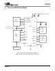
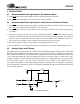
CS4392 2. TYPICAL CONNECTION DIAGRAMS 10 Mode Select 9 (Control Port) * 8 7 +5V Analog + 1.0 µ f 0.1 µf 17 VA M0 (AD0/CS) M1 (SDA/CDIN) M2 (SCL/CCLK) FILT+ 11 0.1 µf + 10 µf M3 CS4392 Logic Power +5V to 1.8V 2 0.1 µf 19 AMUTEC 20 5 Audio Data Processor * AOUTA- VL 4 3 1 6 AOUTA+ LRCK 18 Analog Conditioning & Mute SCLK AOUTB- SDATA Analog BMUTEC 13 AOUTB+ 15 RST MCLK 14 CMOUT Conditioning & Mute 12 AGND 16 + 1.0 µf External Clock Figure 1.
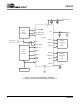
CS4392 0.1 µf + 1.0 µ f +5V Analog 17 VA 10 Mode Select (Control Port) M0 (AD0/CS) 9 M1 (SDA/ CDIN) 8 M2 (SCL/CCLK) FILT+ 11 0.1 µf + 10 µf CS4392 Logic Power +5V to 1.8V 2 0.1 µf 5 7 Audio Data Processor * 4 3 1 6 AOUTAVL 19 Analog AMUTEC 20 AOUTA+ 18 DSD_MODE Conditioning & Mute DSD_CLK DSD_B AOUTB- 14 Analog DSD_A RST BMUTEC 13 AOUTB+ 15 MCLK CMOUT Conditioning & Mute 12 AGND + 1.0 µf 16 External Clock Figure 2.
CS4392 3. APPLICATIONS 3.1 Recommended Power-up Sequence for Hardware Mode 1) Hold RST low until the power supplies, master, and left/right clocks are stable. 2) Bring RST high. After 10ms the device will begin normal operation. 3.2 Recommended Power-up Sequence and Access to Control Port Mode 1) Hold RST low until the power supply, master, and left/right clocks are stable. In this state, the control port is reset to its default settings and FILT+ will remain low. 2) Bring RST high.
CS4392 3.4 Interpolation Filter To accommodate the increasingly complex requirements of digital audio systems, the CS4392 incorporates selectable interpolation filters for each mode of operation. A fast and a slow roll-off filter is available in each of Single, Double, and Quad Speed modes. These filters have been designed to accommodate a variety of musical tastes and styles. Bit 5 of the Mode Control 3 register (06h) is used to select which filter is used.
CS4392 3.6 Digital Interface Format The device will accept audio samples in several digital interface formats as illustrated in Tables 5 and 8. The desired format is selected via the M0 and M1 pins for stand alone mode, and through the DIF2:0 bits in the control port. For an illustration of the required relationship between the Left/Right Clock, Serial Clock and Serial Audio Data, see Figures 4-6.
CS4392 3.7 De-Emphasis The device includes on-chip digital de-emphasis. Figure 7 shows the de-emphasis curve for FS equal to 44.1 kHz. The frequency response of the de-emphasis curve will scale proportionally with changes in sample rate, Fs. Please see Table 5 for the desired de-emphasis control for Stand-alone mode and Table 10 for control port mode. The de-emphasis feature is included to accommodate audio recordings that utilize 50/15 µS pre-emphasis equalization as a means of noise reduction.
CS4392 3.9 Using DSD mode In stand-alone mode, DSD operation is selected by holding DSD_EN(LRCK) high and applying the DSD data and clocks to the appropriate pins. The M2:0 pins set the expected DSD rate and MCLK ratio. In control-port mode the FM bits set the device into DSD mode (DSD_EN pin is not required to be held high). The DIF register then controls the expected DSD rate and MCLK ratio.
CS4392 4. CONTROL PORT INTERFACE The control port is used to load all the internal register settings (see section 6). The operation of the control port may be completely asynchronous with the audio sample rate. However, to avoid potential interference problems, the control port pins should remain static if no operation is required. The control port operates in one of two modes: I2C or SPI. Notes: MCLK must be applied during all I2C communication. 4.0.
CS4392 4.0.2b I2C Read To read from the device, follow the procedure below while adhering to the control port Switching Specifications. 1) Initiate a START condition to the I2C bus followed by the address byte. The upper 6 bits must be 001000. The seventh bit must match the setting of the AD0 pin, and the eighth must be 1. The eighth bit of the address byte is the R/W bit. 2) After transmitting an acknowledge (ACK), the device will then transmit the contents of the register pointed to by the MAP.
CS4392 4.0.3 SPI Mode In SPI mode, data is clocked into the serial control data line, CDIN, by the serial control port clock, CCLK (see Figure 9 for the clock to data relationship). There is no AD0 pin. Pin CS is the chip select signal and is used to control SPI writes to the control port. When the device detects a high to low transition on the AD0/CS pin after power-up, SPI mode will be selected. All signals are inputs and data is clocked in on the rising edge of CCLK. 4.0.
CS4392 5.
CS4392 6. REGISTER DESCRIPTION ** All registers are read/write in Two-Wire mode and write only in SPI mode, unless otherwise noted** 6.1 Mode Control 1 - Address 01h 7 AMUTE 6.1.1 6 DIF2 5 DIF1 4 DIF0 3 DEM1 2 DEM0 1 FM1 0 FM0 Auto-Mute (Bit 7) Function: The Digital-to-Analog converter output will mute following the reception of 8192 consecutive audio samples of static 0 or -1. A single sample of non-static data will release the mute.
CS4392 DSD Mode - The relationship between the oversampling ratio of the DSD audio data and the required Master clock to DSD data rate is defined by the Digital interface Format pins. Note that the Functional Mode registers must be set to DSD Mode. See 9 for register options.
CS4392 6.2 Volume and Mixing Control (Address 02h) 7 A=B 6 Soft 6.2.1 5 Zero Cross 4 ATAPI4 3 ATAPI3 2 ATAPI2 1 ATAPI1 0 ATAPI0 Channel A Volume = Channel B Volume (Bit 7) Function: The AOUTA and AOUTB volume levels are independently controlled by the A and the B Channel Volume Control Bytes when this function is disabled. The volume on both AOUTA and AOUTB are determined by the A Channel Volume Control Byte and the B Channel Byte is ignored when this function is enabled. 6.2.
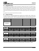
CS4392 ATAPI4 0 0 0 0 0 0 0 0 0 0 0 0 0 0 0 0 1 1 1 1 1 1 1 1 1 1 1 1 1 1 1 1 ATAPI3 0 0 0 0 0 0 0 0 1 1 1 1 1 1 1 1 0 0 0 0 0 0 0 0 1 1 1 1 1 1 1 1 ATAPI2 0 0 0 0 1 1 1 1 0 0 0 0 1 1 1 1 0 0 0 0 1 1 1 1 0 0 0 0 1 1 1 1 ATAPI1 0 0 1 1 0 0 1 1 0 0 1 1 0 0 1 1 0 0 1 1 0 0 1 1 0 0 1 1 0 0 1 1 ATAPI0 0 1 0 1 0 1 0 1 0 1 0 1 0 1 0 1 0 1 0 1 0 1 0 1 0 1 0 1 0 1 0 1 AOUTA MUTE MUTE MUTE MUTE aR aR aR aR aL aL aL aL a[(L+R)/2] a[(L+R)/2] a[(L+R)/2] a[(L+R)/2] MUTE MUTE MUTE MUTE aR aR aR aR aL aL aL aL [(aL+bR
CS4392 6.3 Channel A Volume Control - Address 03h See 4.4 Channel B Volume Control - Address 04h 6.4 CHANNEL B VOLUME CONTROL - ADDRESS 04H 7 MUTE 6.4.1 6 VOL6 5 VOL5 4 VOL4 3 VOL3 2 VOL2 1 VOL1 0 VOL0 Mute (Bit 7) Function: The Digital-to-Analog converter output will mute when enabled. The common mode voltage on the output will be retained. The muting function is effected, similiar to attenuation changes, by the Soft and Zero Cross bits in the Volume and Mixing Control register.
CS4392 6.5.2 Control Port Enable (Bit 5) Function: This bit defaults to 0, allowing the device to power-up in Stand-Alone mode. The Control port mode can be accessed by setting this bit to 1. This will allow the operation of the device to be controlled by the registers and the pin definitions will conform to Control Port Mode. To accomplish a clean powerup, the user should write 30h to register 5 within 10 ms following the release of Reset. 6.5.
CS4392 6.6.2 Soft Volume Ramp-up after Reset (Bit 3) Function: This function allows the user to control whether a soft ramp up in volume is applied when reset is released either by the reset pin or internal to the chip. The modes are as follows: 0 - An instantaneous change is made from max attenuation to the control port volume setting on release of reset (default setting). 1 - Volume is ramped up using the soft-ramp settings in Bits 6:5 of register 02h (see 6.2.
CS4392 7. CHARACTERISTICS/SPECIFICATIONS ANALOG CHARACTERISTICS (CS4392-KS/KZ/KZZ) ((Test conditions (unless otherwise specified): Input test signal is a 997 Hz sine wave at 0 dBFS; measurement bandwidth is 10 Hz to 20 kHz; test load RL = 3kΩ, CL = 10 pF. Typical performance characteristics are derived from measurements taken at TA = 25 °C, VL = VA = 5.0V. Min/Max performance characteristics are guaranteed over the specified operating temperature and voltages.) VA = 5.
CS4392 COMBINED INTERPOLATION & ON-CHIP ANALOG FILTER RESPONSE (The filter characteristics and the X-axis of the response plots have been normalized to the sample rate (Fs) and can be referenced to the desired sample rate by multiplying the given characteristic by Fs.) Parameter Single-Speed Mode - (4 kHz to 50 kHz sample rates) Passband to -0.
CS4392 COMBINED INTERPOLATION & ON-CHIP ANALOG FILTER RESPONSE (Cont.) Parameter Single-Speed Mode - (4 kHz to 50 kHz sample rates) Passband to -0.01 dB corner to -3 dB corner Frequency Response 10 Hz to 20 kHz StopBand StopBand Attenuation (Note 4) Group Delay Passband Group Delay Deviation 0 - 20 kHz De-emphasis Error (Relative to 1kHz) Fs = 32 kHz (Note 5) Fs = 44.1 kHz Fs = 48 kHz Double-Speed Mode - (50 kHz to 100 kHz sample rates) Passband to -0.
CS4392 0 20 20 40 40 Amplitude (dB) Amplitude (dB) 0 60 60 80 80 100 100 120 120 0.4 0.5 0.6 0.7 0.8 Frequency(normalized to Fs) 0.9 1 Figure 12. Single Speed (fast) Stopband Rejection 0.4 0.42 0.44 0.46 0.48 0.5 0.52 Frequency(normalized to Fs) 0.54 0.56 0.58 0.6 Figure 13. Single Speed (fast) Transition Band 0.02 0 1 0.015 2 0.01 0.005 4 Amplitude (dB) Amplitude (dB) 3 5 6 0 0.005 7 0.01 8 0.015 9 10 0.45 0.46 0.47 0.48 0.49 0.5 0.
CS4392 0.02 0 1 0.015 2 0.01 3 Amplitude (dB) Amplitude (dB) 0.005 4 5 6 0 0.005 7 0.01 8 0.015 9 10 0.45 0.02 0.46 0.47 0.48 0.49 0.5 0.51 Frequency(normalized to Fs) 0.52 0.53 0.54 0.55 Figure 18. Single Speed (slow) Transition Band (detail) 0.1 0.15 0.2 0.25 0.3 Frequency(normalized to Fs) 0.35 0.4 0.45 0.5 0 20 20 40 40 Amplitude (dB) Amplitude (dB) 0.05 Figure 19. Single Speed (slow) Passband Ripple 0 60 60 80 80 100 100 120 0 120 0.4 0.5 0.6 0.
CS4392 0 20 20 40 40 Amplitude (dB) Amplitude (dB) 0 60 60 80 80 100 100 120 120 0.2 0.3 0.4 0.5 0.6 0.7 Frequency(normalized to Fs) 0.8 0.9 1 Figure 24. Double Speed (slow) Stopband Rejection 0.2 0.3 0.4 0.5 0.6 Frequency(normalized to Fs) 0.7 0.8 Figure 25. Double Speed (slow) Transition Band 0 0.02 1 0.015 2 0.01 0.005 4 Amplitude (dB) Amplitude (dB) 3 5 6 0 0.005 7 0.01 8 0.015 9 10 0.45 0.46 0.47 0.48 0.49 0.5 0.51 Frequency(normalized to Fs) 0.52 0.
CS4392 0.2 0 1 0.15 2 0.1 3 Amplitude (dB) Amplitude (dB) 0.05 4 5 6 0 0.05 7 0.1 8 0.15 9 10 0.45 0.2 0.46 0.47 0.48 0.49 0.5 0.51 Frequency(normalized to Fs) 0.52 0.53 0.54 0.55 Figure 30. Quad Speed (fast) Transition Band (detail) 0 0.05 0.1 0.15 Frequency(normalized to Fs) 0.2 0.25 Figure 31. Quad Speed (fast) Passband Ripple 0 0 20 40 40 Amplitude (dB) Amplitude (dB) 20 60 60 80 80 100 100 120 120 0.1 0.2 0.3 0.4 0.5 0.6 0.
CS4392 SWITCHING CHARACTERISTICS - SERIAL AUDIO INTERFACE (Inputs: Logic 0 = 0 V, Logic 1 = VL) .
CS4392 SWITCHING SPECIFICATIONS - DSD INTERFACE (Logic 0 = AGND; Logic 1 = VL) Parameter Symbol Min 40 Max 60 Unit % DSD_SCLK Pulse Width Low DSD_SCLK Pulse Width High DSD_SCLK Period tsclkl tsclkh tsclkw 20 20 20 - ns ns ns DSD_L or DSD_R valid to DSD_SCLK rising setup time DSD_SCLK rising to DSD_L or DSD_R hold time tsdlrs tsdh 20 20 - ns ns MCLK Duty Cycle t sclkh t sclkl D S D _S C LK t sdlrs t sdh D SD_L, DSD_R Figure 37.
CS4392 SWITCHING CHARACTERISTICS - CONTROL PORT INTERFACE (Inputs: logic 0 = AGND, logic 1 = VL) Parameter Symbol Min Max Unit SCL Clock Frequency fscl - 100 kHz RST Rising Edge to Start tirs 500 - ns Bus Free Time Between Transmissions tbuf 4.7 - µs Start Condition Hold Time (prior to first clock pulse) thdst 4.0 - µs Clock Low time tlow 4.7 - µs Clock High Time thigh 4.0 - µs Setup Time for Repeated Start Condition tsust 4.
CS4392 SWITCHING CHARACTERISTICS - SPI CONTROL PORT (Inputs: logic 0 = AGND, logic 1 = VL) Parameter Symbol Min Max Unit CCLK Clock Frequency fsclk - 6 MHz RST Rising Edge to CS Falling tsrs 500 - ns tspi 500 - ns CS High Time Between Transmissions tcsh 1.
CS4392 DC ELECTRICAL CHARACTERISTICS (AGND = 0V; all voltages with respect to AGND.) Parameter Normal Operation (Note 10) Power Supply Current Power Dissipation Power-Down Mode (Note 11) Power Supply Current Power Dissipation All Modes of Operation Power Supply Rejection Ratio (Note 12) Symbol Min Typ Max Units All Supplies=5.0V IA + IL - 26 130 30 150 mA mW All Supplies=5.0V IA + IL - 300 1.5 - µA mW (1 kHz) (60 Hz) PSRR - 60 40 0.48•VA 250 0.001 - dB dB V - VA 250 0.
CS4392 RECOMMENDED OPERATING SPECIFICATIONS (AGND = 0V; all voltages with respect to AGND.) Parameters DC Power Supply Symbol VA VL Min 4.75 1.8 Typ 5.0 - Max 5.25 VA Units V V ABSOLUTE MAXIMUM RATINGS (AGND = 0 V; all voltages with respect to ground.) Parameters DC Power Supply Input Current, Any Pin Except Supplies Digital Input Voltage Ambient Operating Temperature (power applied) Storage Temperature Symbol VA VL Iin VIND TA Tstg Min -0.3 -0.3 -0.3 -55 -65 Max 6.0 VA ±10 VL+0.
CS4392 8. PARAMETER DEFINITIONS Total Harmonic Distortion + Noise (THD+N) The ratio of the rms value of the signal to the rms sum of all other spectral components over the specified bandwidth (typically 10Hz to 20kHz), including distortion components. Expressed in decibels. Dynamic Range The ratio of the full scale rms value of the signal to the rms sum of all other spectral components over the specified bandwidth.
CS4392 10.PACKAGE DIMENSIONS 20L TSSOP (4.4 mm BODY) PACKAGE DRAWING N D E11 A2 E A ∝ e b2 SIDE VIEW A1 END VIEW L SEATING PLANE 1 2 3 TOP VIEW INCHES DIM A A1 A2 b D E E1 e L ∝ MIN -0.002 0.03346 0.00748 0.252 0.248 0.169 -0.020 0° NOM -0.004 0.0354 0.0096 0.256 0.2519 0.1732 -0.024 4° NOT E MILLIMETERS MAX 0.043 0.006 0.037 0.012 0.259 0.256 0.177 0.026 0.028 8° MIN -0.05 0.85 0.19 6.40 6.30 4.30 -0.50 0° NOM --0.90 0.245 6.50 6.40 4.40 -0.60 4° MAX 1.10 0.15 0.95 0.30 6.60 6.50 4.
CS4392 PACKAGE DIMENSIONS(cont.). 20L SOIC (300 MIL BODY) PACKAGE DRAWING E H 1 b c ∝ D L SEATING PLANE A e DIM A A1 b C D E e H L ∝ MIN 0.093 0.004 0.013 0.009 0.496 0.291 0.040 0.394 0.016 0° A1 INCHES NOM 0.098 0.008 0.017 0.011 0.504 0.295 0.050 0.407 0.025 4° MAX 0.104 0.012 0.020 0.013 0.512 0.299 0.060 0.419 0.050 8° MIN 2.35 0.10 0.33 0.23 12.60 7.40 1.02 10.00 0.40 0° MILLIMETERS NOM 2.50 0.20 0.43 0.28 12.80 7.50 1.27 10.34 0.64 4° MAX 2.65 0.30 0.51 0.32 13.00 7.60 1.52 10.65 1.