
Manual

CS4391
DS335PP4 11
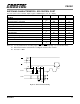
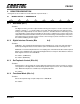
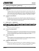
SWITCHING CHARACTERISTICS - SPI CONTROL PORT
(T
A
= 25° C; VL = 5.5 to 1.8 Volts; Inputs: logic 0 = AGND, logic 1 = VL, C
L
= 30 pF)
Notes: 24. t
spi
only needed before first falling edge of CS after RST rising edge. t
spi
= 0 at all other times.
25. Data must be held for sufficient time to bridge the transition time of CCLK.
26. For F
SCK
< 1 MHz
Parameter Symbol Min Max Unit
SPI Mode
CCLK Clock Frequency f
sclk
-6MHz
RST
Rising Edge to CS Falling t
srs
500 - ns
CCLK Edge to CS
Falling (Note 24) t
spi
500 - ns
CS
High Time Between Transmissions t
csh
1.0 - µs
CS
Falling to CCLK Edge t
css
20 - ns
CCLK Low Time t
scl
66 - ns
CCLK High Time t
sch
66 - ns
CDIN to CCLK Rising Setup Time t
dsu
40 - ns
CCLK Rising to DATA Hold Time (Note 25) t
dh
15 - ns
Rise Time of CCLK and CDIN (Note 26) t
r2
- 100 ns
Fall Time of CCLK and CDIN (Note 26) t
f2
- 100 ns
t
r2
t
f2
t
dsu
t
dh
t
sch
t
scl
CS
CCLK
CDIN
t
css
t
csh
t
spi
t
srs
RST
Figure 4. SPI Control Port Timing