CS4391 24-Bit, 192 kHz Stereo DAC with Volume Control Features Description Complete Stereo DAC System: Interpolation, D/A, Output Analog Filtering 108 dB Dynamic Range 94 dB THD+N Direct Stream Digital Mode Low Clock Jitter Sensitivity +5 V to +3 V Power Supply ATAPI Mixing On-Chip Digital De-emphasis for 32, 44.
CS4391 TABLE OF CONTENTS 1. CHARACTERISTICS/SPECIFICATIONS .......................................................................... 5 ANALOG CHARACTERISTICS...................................................................................... 5 DIGITAL CHARACTERISTICS....................................................................................... 7 ABSOLUTE MAXIMUM RATINGS ................................................................................. 7 RECOMMENDED OPERATING CONDITIONS...........
CS4391 Serial Audio Data - SDATA ...........................................................................................21 Serial Clock - SCLK ......................................................................................................22 Left / Right Clock - LRCK ..............................................................................................22 Master Clock - MCLK ....................................................................................................
CS4391 LIST OF TABLES Figure:1. Digital Interface Formats - PCM Modes ....................................................................... 26 Figure:2. Digital Interface Formats - DSD Mode ......................................................................... 26 Figure:3. De-Emphasis Mode Selection ..................................................................................... 26 Figure:4. Functional Mode Selection .................................................................................
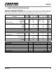
CS4391 1. CHARACTERISTICS/SPECIFICATIONS ANALOG CHARACTERISTICS (TA = 25° C; Logic "1" = VL = VA; Logic "0" = AGND; Full-Scale Output Sine Wave, 997 Hz; MCLK = 12.288 MHz; SCLK = 3.072 MHz, Sample Rate = 48, 96 or 192 kHz, 24-bit data, Measurement Bandwidth 10 Hz to 20 kHz, unless otherwise specified.
CS4391 ANALOG CHARACTERISTICS (continued) Parameter Symbol Min Typ Max Combined Digital and On-chip Analog Filter Response - Single Speed Mode Passband (Note 3) to -0.05 dB corner 0 .4535 to -3 dB corner 0 .4998 Frequency Response 10 Hz to 20 kHz -.02 +.035 StopBand .5465 StopBand Attenuation (Note 5) 50 Group Delay tgd 9/Fs Passband Group Delay Deviation 0 - 20 kHz ±0.36/Fs De-emphasis Error (Relative to 1 kHz) +.2/-.1 Control Port Mode Fs = 32 kHz +.05/-.14 Fs = 44.1 kHz +0/.
CS4391 DIGITAL CHARACTERISTICS (TA = 25° C) Parameters High-Level Input Voltage Low-Level Input Voltage Input Leakage Current Input Capacitance Maximum MUTEC Drive Current Symbol VIH Min 70% VIL Iin - Typ - Max - Units VL - 20% VL 8 3 ±10 - µA pF mA ABSOLUTE MAXIMUM RATINGS (AGND = 0 V; all voltages with respect to ground.
CS4391 SWITCHING CHARACTERISTICS - PCM MODES (TA = -10 to 70° C; VL = 5.5 to 1.
CS4391 SWITCHING CHARACTERISTICS - DSD (TA= -10 to 70° C; Logic 0 = AGND = DGND; Logic 1 = VL = 5.5 to 1.8 Volts; CL = 20 pF) Parameter Symbol Min 40 Typ 50 Max 60 Unit % SCLK Pulse Width Low SCLK Pulse Width High SCLK Period tsclkl tsclkh tsclkw TBD TBD TBD - - ns ns ns SDIN valid to SCLK rising setup time SCLK rising to SDIN hold time tsdlrs tsdh TBD TBD - - ns ns MCLK Duty Cycle t sclkh t sclkl S C LK t s dlrs t sd h S D A TA Figure 2.
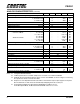
CS4391 SWITCHING CHARACTERISTICS - I2C CONTROL PORT (TA = 25° C; VL = 5.5 to 1.8 Volts; Inputs: logic 0 = AGND, logic 1 = VL, C L = 30 pF) Parameter Symbol Min Max Unit SCL Clock Frequency fscl - 100 KHz RST Rising Edge to Start tirs 500 - ns Bus Free Time Between Transmissions tbuf 4.7 - µs Start Condition Hold Time (prior to first clock pulse) thdst 4.0 - µs Clock Low time tlow 4.7 - µs Clock High Time thigh 4.0 - µs Setup Time for Repeated Start Condition tsust 4.
CS4391 SWITCHING CHARACTERISTICS - SPI CONTROL PORT (TA = 25° C; VL = 5.5 to 1.8 Volts; Inputs: logic 0 = AGND, logic 1 = VL, C L = 30 pF) Parameter Symbol Min Max Unit CCLK Clock Frequency fsclk - 6 MHz RST Rising Edge to CS Falling tsrs 500 - ns tspi 500 - ns CS High Time Between Transmissions tcsh 1.
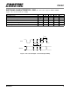
CS4391 2. TYPICAL CONNECTION DIAGRAMS 0.1 µf 10 Mode Select (Control Port) * 9 8 7 +1.0 µ f +5V to +3V Analog 17 VA M0 (AD0/CS) M1 (SDA/CDIN) FILT+ 11 M2 (SCL/CCLK) 0.1 µf + 1.0 µf M3 CS4391 Logic Power +5V to 1.8V 2 0.1 µf 19 AMUTEC 20 5 Audio Data Processor * AOUTA- VL 4 3 1 6 AOUTA+ 18 LRCK Analog Conditioning & Mute SCLK AOUTB- SDATA 14 BMUTEC 13 RST AOUTB+ 15 Analog Conditioning & Mute CMOUT 12 MCLK AGND 16 + 1.0 µf External Clock Figure 5.
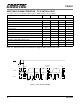
CS4391 0.1 µf +1.0 µ f +5V to +3V Analog 17 VA Mode Select (Control Port) 10 M0 (AD0/CS) 9 M1 (SDA/CDIN) 8 M2 (SCL/CCLK) FILT+ 11 0.1 µf + 1.0 µf CS4391 Logic Power +5V to 1.8V 2 0.1 µf 5 7 Audio Data Processor * 4 3 AOUTAVL 19 AMUTEC 20 DSD_MODE AOUTA+ 18 Analog Conditioning & Mute DSD_CLK DSD_B AOUTBDSD_A 1 RST 6 MCLK 14 BMUTEC 13 AOUTB+ 15 Analog Conditioning & Mute CMOUT 12 AGND 16 + 1.0 µf External Clock Figure 6.
CS4391 3. REGISTER QUICK REFERENCE ** “default” ==> bit status after power-up-sequence or reset** 3.1 MODE CONTROL 1 (ADDRESS 01H) 7 AMUTE 1 6 DIF2 0 5 DIF1 0 4 DIF0 0 3 DEM1 0 2 DEM0 0 1 FM1 0 0 FM0 0 AMUTE (Auto-mute) Default = ‘1’. 0 - Disabled 1 - Enabled DIF2, DIF1 and DIF0 (Digital Interface Format - PCM Modes). See Table 1 Default = ‘0’.
CS4391 3.2 VOLUME AND MIXING CONTROL (ADDRESS 02H) 7 A=B 0 6 Soft 1 5 Zero Cross 0 4 ATAPI4 0 3 ATAPI3 1 2 ATAPI2 0 1 ATAPI1 0 0 ATAPI0 1 A = B (Channel A Volume = Channel B Volume) Default = ‘0’. 0 - AOUTA volume is determined by register 03h and AOUTB volume is determined by register 04h. 1 - AOUTA and AOUTB volumes are determined by register 03h and register 04h is ignored. Soft & Zero Cross (Soft control and zero cross detection control) Default = ‘10’.
CS4391 3.5 MODE CONTROL 2 (ADDRESS 05H) 7 INVERT_A 0 6 INVERT_B 0 5 CPEN 1 4 PDN 1 3 MUTEC A = B 0 2 FREEZE 0 1 MCLK Divide 0 0 Reserved 0 INVERT_A (Invert Channel A) Default = ‘0’. 0 - Disabled 1 - Enabled INVERT_B (Invert Channel B) Default = ‘0’. 0 - Disabled 1 - Enabled CPEN (Control Port Enable) Default = ‘0’ 0 - Disabled (Stand-Alone Mode) 1 - Enabled (Control Port Mode) PDN (Power-Down) Default =’1’. 0 - Disabled 1 - Enabled MUTEC A=B Default = ‘0’.
CS4391 4. REGISTER DESCRIPTION ** All register access is R/W in I2C mode and write only in SPI mode ** 4.1 MODE CONTROL 1 - ADDRESS 01H 7 AMUTE 4.1.1 6 DIF2 5 DIF1 4 DIF0 3 DEM1 2 DEM0 1 FM1 0 FM0 Auto-Mute (Bit 7) Function: The Digital-to-Analog converter output will mute following the reception of 8192 consecutive audio samples of static 0 or -1. A single sample of non-static data will release the mute. Detection and muting is done independently for each channel.
CS4391 4.2 VOLUME AND MIXING CONTROL (ADDRESS 02H) 7 A=B 4.2.1 6 Soft 5 Zero Cross 4 ATAPI4 3 ATAPI3 2 ATAPI2 1 ATAPI1 0 ATAPI0 Channel A Volume = Channel B Volume (Bit 7) Function: The AOUTA and AOUTB volume levels are independently controlled by the A and the B Channel Volume Control Bytes when this function is disabled. The volume on both AOUTA and AOUTB are determined by the A Channel Volume Control Byte and the B Channel Byte is ignored when this function is enabled. 4.2.
CS4391 4.4 CHANNEL B VOLUME CONTROL - ADDRESS 04H 7 MUTE 4.4.1 6 VOL6 5 VOL5 4 VOL4 3 VOL3 2 VOL2 1 VOL1 0 VOL0 Mute (Bit 7) Function: The Digital-to-Analog converter output will mute when enabled. The common mode voltage on the output will be retained. The muting function is effected, similiar to attenuation changes, by the Soft and Zero Cross bits in the Volume and Mixing Control register. The MUTEC pin for that channel will go active during the mute period if the Mute function is enabled.
CS4391 4.5.5 Freeze (Bit 2) Function: This function allows modifications to the registers without the changes being taking effect until Freeze is disabled. To make multiple changes in the Control port registers take effect simultaneously, set the Freeze Bit, make all register changes, then Disable the Freeze bit. 4.5.6 Master Clock Divide (Bit 1) Function: This function allows the user to select an internal divide by 2 of the Master Clock.
CS4391 5.
CS4391 Serial Clock - SCLK Pin 4, Input Function: Clocks the individual bits of the serial data into the SDATA pin. The required relationship between the Left/Right clock, serial clock and serial data is defined by the Mode Control Byte in Control Port Mode or the Mode pins in Hardware Mode. The options are detailed in Figures 7-24. Left / Right Clock - LRCK Pin 5, Input Function: The Left / Right clock determines which channel is currently being input on the serial audio data input, SDATA.
CS4391 Serial Control Interface Clock - SCL/CCLK (Control Port Mode) Pin 8, Input Function: Clocks the serial control data into or from SDA/CDIN. Serial Control Data I/O - SDA/CDIN (Control Port Mode) Pin 9, Input/Output Function: In I2C mode, SDA is a data I/O line. CDIN is the input data line for the control port interface in SPI mode. Address Bit / Chip Select - AD0 / CS (Control Port Mode) Pin 10, Input Function: In I2C mode, AD0 is a chip address bit.
CS4391 Differential Analog Output - AOUTB+, AOUTB- and AOUTA+, AOUTAPins 14, 15 and 18, 19, Outputs Function: The full scale differential analog output level is specified in the Analog Characteristics specifications table. Analog Ground - AGND Pin 16, Input Function: Analog ground reference. Analog Power - VA Pin 17, Input Function: Analog power supply. Typically 3 to 5 VDC.
CS4391 6.
CS4391 DIF2 0 0 DIF1 0 0 DIFO 0 1 0 0 1 1 1 1 1 1 0 0 1 1 0 1 0 1 0 1 DESCRIPTION Left Justified, up to 24-bit data I2S, up to 24-bit data Right Justified, 16-bit Right Justified, 24-bit Right Justified, 20-bit Right Justified, 18-bit Reserved Reserved Data Data Data Data Table 1.
CS4391 ATAPI4 0 0 0 0 0 0 0 0 0 0 0 0 0 0 0 0 1 1 1 1 1 1 1 1 1 1 1 1 1 1 1 1 ATAPI3 0 0 0 0 0 0 0 0 1 1 1 1 1 1 1 1 0 0 0 0 0 0 0 0 1 1 1 1 1 1 1 1 ATAPI2 0 0 0 0 1 1 1 1 0 0 0 0 1 1 1 1 0 0 0 0 1 1 1 1 0 0 0 0 1 1 1 1 ATAPI1 0 0 1 1 0 0 1 1 0 0 1 1 0 0 1 1 0 0 1 1 0 0 1 1 0 0 1 1 0 0 1 1 ATAPI0 0 1 0 1 0 1 0 1 0 1 0 1 0 1 0 1 0 1 0 1 0 1 0 1 0 1 0 1 0 1 0 1 AOUTA MUTE MUTE MUTE MUTE aR aR aR aR aL aL aL aL a[(L+R)/2] a[(L+R)/2] a[(L+R)/2] a[(L+R)/2] MUTE MUTE MUTE MUTE aR aR aR aR aL aL aL aL [(aL+b
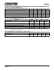
CS4391 Note:These clocking ratios are only available inControl Port Mode when the MCLK Divide bit is enabled. Sample Rate (kHz) MCLK (MHz) 384x 512x 12.2880 16.3840 16.9344 22.5792 18.4320 24.5760 256x 8.1920 11.2896 12.2880 32 44.1 48 See Note 1024x 32.7680 45.1584 49.1520 768x 24.5760 33.8688 36.8640 Table 8. Single Speed (4 to 50 kHz sample rates) Common Clock Frequencies Sample Rate (kHz) MCLK (MHz) 192x 256x 12.2880 16.3840 16.9344 22.5792 18.4320 24.5760 128x 8.1920 11.2896 12.2880 64 88.
CS4391 M3 1 1 M2 1 1 M1 0 0 M0 0 1 1 1 1 1 1 1 0 1 DESCRIPTION Left Justified up to 24-bit data I2S up to 24-bit data Right Justified 16-bit data Right Justified 24-bit data FORMAT 0 1 FIGURE 7 8 2 3 9 10 Table 14.
CS4391 L eft C ha n n el LRC K R igh t C ha n n el SC L K SDATA M SB -1 -2 -3 -4 -5 +5 +4 +3 +2 +1 LS B M SB -1 -2 -3 -4 +5 +4 +3 +2 +1 LSB Figure 7. Format 0, Left Justified up to 24-Bit Data L eft C ha n n el LRC K R igh t C ha n n el SC L K SDATA MS B -1 -2 -3 -4 -5 +5 +4 +3 +2 +1 LS B MSB -1 -2 -3 -4 +5 +4 +3 +2 +1 LSB Figure 8.
CS4391 LR C K R ig h t C h a n n e l L e ft C h a n n e l SCLK SDATA 1 0 1 9 1 8 17 16 15 14 1 3 1 2 11 10 9 8 7 6 5 4 3 2 1 0 19 18 17 16 15 14 13 12 11 10 9 8 7 6 5 4 3 2 1 0 3 2 1 0 3 2 cloc4, ks Right Justified 20-Bit Data. (Available in Control Port Mode only) Figure 11. Format LR CK R ig h t C h a n ne l L eft C h a nn e l SCLK SDATA 1 0 17 16 15 14 13 12 11 10 9 8 7 6 5 4 3 2 1 0 17 16 15 14 13 12 11 10 9 8 7 6 5 4 Figure 12.
CS4391 4) The desired register settings can be loaded while keeping the PDN bit set to 1. 7. APPLICATIONS 7.1 Recommended Power-up Sequence for Hardware Mode 5) Set the PDN bit to 0 which will initiate the power-up sequence which requires approximately 10 µS. 1) Hold RST low until the power supplies, master, and left/right clocks are stable. 7.3 2) Bring RST high. 7.
CS4391 8. CONTROL PORT INTERFACE The control port is used to load all the internal settings of the CS4391. The operation of the control port may be completely asynchronous to the audio sample rate. However, to avoid potential interference problems, the control port pins should remain static if no operation is required. The control port has 2 modes: SPI and I2C, with the CS4391 operating as a slave device in both modes. If I2C operation is desired, AD0/CS should be tied to VA or AGND.
CS4391 7 INCR 0 6 Reserved 0 5 Reserved 0 4 Reserved 0 3 Reserved 0 2 MAP2 0 1 MAP1 0 0 MAP0 0 INCR (Auto MAP Increment Enable) Default = ‘0’. 0 - Disabled 1 - Enabled MAP0-2 (Memory Address Pointer) Default = ‘000’. Table 16. Memory Address Pointer (MAP) CS CCLK C H IP ADDRESS C DIN 0 01 00 0 0 MAP DATA MSB R/W b yte 1 LS B b yte n M AP = M e m ory Ad d re ss P o in te r Figure 16.
CS4391 0.25 0.2 0.15 Amplitude dB 0.1 0.05 0 -0.05 -0.1 -0.15 -0.2 -0.25 0 0.05 0.1 0.15 0.2 0.25 0.3 0.35 0.4 0.45 0.5 Frequency (normalized to Fs) Figure 18. Single-Speed Frequency Response Figure 19. Single-Speed Transition Band Figure 20. Single-Speed Transition Band Figure 21. Single-Speed Stopband Rejection 0.25 0.2 0.15 Amplitude dB 0.1 0.05 0 -0.05 -0.1 -0.15 -0.2 -0.25 0 0.05 0.1 0.15 0.2 0.25 0.3 0.35 0.4 0.45 0.5 Frequency (norm alized to Fs) Figure 22.
CS4391 Figure 24. Double-Speed Transition Band 36 Figure 25.
CS4391 9. PARAMETER DEFINITIONS Total Harmonic Distortion + Noise (THD+N) The ratio of the rms value of the signal to the rms sum of all other spectral components over the specified bandwidth (typically 10Hz to 20kHz), including distortion components. Expressed in decibels. Dynamic Range The ratio of the full scale rms value of the signal to the rms sum of all other spectral components over the specified bandwidth.
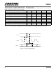
CS4391 11. PACKAGE DIMENSIONS 20L TSSOP (4.4 mm BODY) PACKAGE DRAWING N D E11 A2 E A ∝ e b2 SIDE VIEW A1 END VIEW L SEATING PLANE 1 2 3 TOP VIEW INCHES DIM A A1 A2 b D E E1 e L ∝ MIN -0.002 0.03346 0.00748 0.252 0.248 0.169 -0.020 0° NOM -0.004 0.0354 0.0096 0.256 0.2519 0.1732 -0.024 4° MILLIMETERS MAX 0.043 0.006 0.037 0.012 0.259 0.256 0.177 0.026 0.028 8° MIN -0.05 0.85 0.19 6.40 6.30 4.30 -0.50 0° NOM --0.90 0.245 6.50 6.40 4.40 -0.60 4° NOT E MAX 1.10 0.15 0.95 0.30 6.60 6.50 4.