
User Manual


DS671F2 15
CS4385
SWITCHING CHARACTERISTICS - PCM
Inputs: Logic 0 = GND, Logic 1 = VLS, C
L
= 20 pF.
Notes:
14. After powering up, RST
should be held low until after the power supplies and clocks are settled.
15. See Tables 1 - 3 for suggested MCLK frequencies.
16. Not valid for TDM Mode.
17. MSB of CH1 is always the second SCLK rising edge following LRCK rising edge.
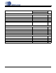
Parameters Symbol Min Max Units
RST pin Low Pulse Width (Note 14) 1-ms
MCLK Frequency 1.024 55.2 MHz
MCLK Duty Cycle (Note 15) 45 55 %
Input Sample Rate - LRCK (Manual selection) Single-Speed Mode
Double-Speed Mode
Quad-Speed Mode
F
s
F
s
F
s
4
50
100
54
108
216
kHz
kHz
kHz
Input Sample Rate - LRCK (Auto detect) Single-Speed Mode
Double-Speed Mode
Quad-Speed Mode
Fs
Fs
Fs
4
84
170
54
108
216
kHz
kHz
kHz
LRCK Duty Cycle (Note 16) 45 55 %
SCLK Duty Cycle 45 55 %
SCLK High Time t
sckh
8-ns
SCLK Low Time t
sckl
8-ns
LRCK Edge to SCLK Rising Edge t
lcks
5-ns
SCLK Rising Edge to LRCK Falling Edge t
lckd
5-ns
TDM LRCK hightime pulse (Note 17) t
lpw
1/f
SCLK
7/f
SCLK
ns
SDIN Setup Time Before SCLK Rising Edge t
ds
3-ns
SDIN Hold Time After SCLK Rising Edge t
dh
5-ns
SDINx
t
ds
SCLK
LRCK
MSB
t
dh
t
sckh
t
sckl
t
lcks
MSB-1
Figure 1. Serial Audio Interface Timing
sckh
sckl
t
t
SDIN1
dh
t
ds
t
SCLK
LRCK
lcks
t
MSB MSB-1
lp w
t
lcks
t
lckd
t
Figure 2. TDM Serial Audio Interface Ti ming