CS4385 114 dB, 192 kHz 8-Channel D/A Converter Features Description Advanced Multi-bit Delta Sigma Architecture The CS4385 is a complete 8-channel digital-to-analog system. This D/A system includes digital de-emphasis, half-dB step size volume control, ATAPI channel mixing, selectable fast and slow digital interpolation filters followed by an oversampled, multi-bit delta sigma modulator which includes mismatch-shaping technology that eliminates distortion due to capacitor mismatch.
CS4385 TABLE OF CONTENTS 1. PIN DESCRIPTION ...................................................................................................................... 6 2. CHARACTERISTICS AND SPECIFICATIONS ...................................................................................... 8 RECOMMENDED OPERATING CONDITIONS ..................................................................................... 8 ABSOLUTE MAXIMUM RATINGS ..........................................................................
CS4385 6.2 Mode Control 1 (address 02h) ........................................................................................................ 37 6.2.1 Control Port Enable (CPEN) .................................................................................................. 37 6.2.2 Freeze Controls (FREEZE) ................................................................................................... 37 6.2.3 PCM/DSD Selection (DSD/PCM) .............................................................
CS4385 LIST OF FIGURES Figure 1.Serial Audio Interface Timing ...................................................................................................... 15 Figure 2.TDM Serial Audio Interface Timing ............................................................................................. 15 Figure 3.Direct Stream Digital - Serial Audio Input Timing ........................................................................ 16 Figure 4.
CS4385 LIST OF TABLES Table 1. Single-Speed Mode Standard Frequencies ................................................................................ 21 Table 2. Double-Speed Mode Standard Frequencies ............................................................................... 21 Table 3. Quad-Speed Mode Standard Frequencies ................................................................................. 21 Table 4. PCM Digital Interface Format, Hardware Mode Options ...................................
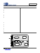
CS4385 AOUTB1- MUTEC1 AOUTA1AOUTA1+ AOUTB1+ DSDA4 DSDB4 VLS DSD_SCLK DSDB2 DSDA3 DSDB3 1.
CS4385 Pin Name AOUTA1 +,AOUTB1 +,AOUTA2 +,AOUTB2 +,AOUTA3 +,AOUTB3 +,AOUTA4 +,AOUTB4 +,- # Pin Description 39, 40 38, 37 35, 36 34, 33 Differential Analog Output (Output) - The full-scale differential analog output level is specified in the 29, 30 Analog Characteristics specification table. 28, 27 25, 26 24, 23 VA 32 Analog Power (Input) - Positive power supply for the analog section. Refer to the Recommended Operating Conditions for appropriate voltages.
CS4385 2. CHARACTERISTICS AND SPECIFICATIONS RECOMMENDED OPERATING CONDITIONS GND = 0 V; all voltages with respect to ground. Parameters Symbol Min Typ Max Units Analog power Digital internal power Serial data port interface power Control port interface power Ambient Operating Temperature (Power Applied) Commercial Grade (-CQZ) Automotive Grade (-DQZ) VA VD VLS VLC 4.75 2.37 1.71 1.71 5.0 2.5 5.0 5.0 5.25 2.63 5.25 5.
CS4385 DAC ANALOG CHARACTERISTICS - COMMERCIAL (-CQZ) Test Conditions (unless otherwise specified): VA = VLS = VLC = 5 V; VD = 2.5 V; TA = 25°C; Full-scale 997 Hz input sine wave (Note 1); Tested under max ac-load resistance; Valid with FILT+ and VQ capacitors as shown in “Typical Connection Diagram” on page 19; Measurement Bandwidth 10 Hz to 20 kHz.
CS4385 DAC ANALOG CHARACTERISTICS - AUTOMOTIVE (-DQZ) Test Conditions (unless otherwise specified): VA = 4.75 to 5.25 V; VLS = 1.71 to 5.25 V; VLC = 1.71 to 5.25 V; VD = 2.37 to 2.63 V; TA = -40°C to 85°C; Full-scale 997 Hz input sine wave (Note 1); Tested under max ac-load resistance; Valid with FILT+ and VQ capacitors as shown in “Typical Connection Diagram” on page 19; Measurement Bandwidth 10 Hz to 20 kHz.
CS4385 POWER AND THERMAL CHARACTERISTICS Parameters Symbol Min Typ Max Units normal operation, VA= 5 V VD= 2.5 V (Note 5) Interface current, VLC=5 V VLS=5 V (Note 6) power-down state (all supplies) Power Dissipation (Note 4) VA = 5 V, VD = 2.
CS4385 COMBINED INTERPOLATION & ON-CHIP ANALOG FILTER RESPONSE The filter characteristics have been normalized to the sample rate (Fs) and can be referenced to the desired sample rate by multiplying the given characteristic by Fs. See Note 12. Fast Roll-Off Parameter Unit Min Typ Max Combined Digital and On-chip Analog Filter Response - Single-Speed Mode - 48 kHz Passband (Note 9) Frequency Response to -0.
CS4385 COMBINED INTERPOLATION & ON-CHIP ANALOG FILTER RESPONSE (CONTINUED) Slow Roll-Off (Note 8) Parameter Unit Min Typ Max 0 0 - 0.417 0.499 Fs Fs -0.01 - +0.01 dB .583 - - Fs 64 - - dB Single-Speed Mode - 48 kHz Passband (Note 9) to -0.01 dB corner to -3 dB corner Frequency Response 10 Hz to 20 kHz StopBand StopBand Attenuation (Note 10) Group Delay De-emphasis Error (Note 11) (Relative to 1 kHz) - 7.8/Fs - s Fs = 32 kHz Fs = 44.1 kHz Fs = 48 kHz - - ±0.36 ±0.21 ±0.
CS4385 DIGITAL CHARACTERISTICS Parameters Input Leakage Current Input Capacitance High-Level Input Voltage Min Typ Max Units Iin 8 - ±10 0.30•VLS 0.30•VLC 0.20•VLC μA pF V V V V V Serial I/O Control I/O Serial I/O Control I/O Control I/O = 3.3 V, 5 V VIH VIH VIL VIL VOL 0.70•VLS 0.70•VLC - Low-Level Output Voltage (IOL = -1.2 mA) Control I/O = 1.8 V, 2.5 V VOL - - 0.
CS4385 SWITCHING CHARACTERISTICS - PCM Inputs: Logic 0 = GND, Logic 1 = VLS, CL = 20 pF. Parameters Symbol RST pin Low Pulse Width (Note 14) MCLK Frequency MCLK Duty Cycle (Note 15) Min Max Units 1 - ms 1.024 55.
CS4385 SWITCHING CHARACTERISTICS - DSD Logic 0 = GND; Logic 1 = VLS; CL = 20 pF. Parameter Symbol MCLK Duty Cycle DSD_SCLK Pulse Width Low DSD_SCLK Pulse Width High DSD_SCLK Frequency tsclkl tsclkh (64x Oversampled) (128x Oversampled) DSD_A / _B valid to DSD_SCLK rising setup time DSD_SCLK rising to DSD_A or DSD_B hold time DSD clock to data transition (Phase Modulation Mode) tsdlrs tsdh tdpm Min Typ Max Unit 40 160 160 1.024 2.048 20 20 -20 - 60 3.2 6.
CS4385 SWITCHING CHARACTERISTICS - CONTROL PORT - I²C FORMAT Inputs: Logic 0 = GND, Logic 1 = VLC, CL = 20 pF. Symbol Min Max Unit SCL Clock Frequency Parameter fscl - 100 kHz RST Rising Edge to Start tirs 500 - ns Bus Free Time Between Transmissions tbuf 4.7 - µs Start Condition Hold Time (prior to first clock pulse) thdst 4.0 - µs Clock Low time tlow 4.7 - µs Clock High Time thigh 4.0 - µs Setup Time for Repeated Start Condition tsust 4.
CS4385 SWITCHING CHARACTERISTICS - CONTROL PORT - SPI FORMAT Inputs: Logic 0 = GND, Logic 1 = VLC, CL = 20 pF. Symbol Min Max Unit CCLK Clock Frequency Parameter fsclk - 6 MHz RST Rising Edge to CS Falling tsrs 500 - ns tspi 500 - ns CS High Time Between Transmissions tcsh 1.
CS4385 3. TYPICAL CONNECTION DIAGRAM +2.5 V +5 V 1 µF + 4 VD AOUTA1AOUTB1+ 6 7 9 PCM Digital Audio Source 8 11 13 14 AOUTB1- MCLK LRCK AOUTA2+ SCLK AOUTA2- SDIN2 AOUTB2+ SDIN3 AOUTB2- AOUTA3- VLS CS4385 0.
CS4385 +2.5 V +5 V 1 µF + 4 VD AOUTA1AOUTB1+ 220 Ω 7 PCM Digital Audio Source 9 8 11 13 14 470 Ω 43 +1.8 V to +5 V AOUTB1- MCLK SCLK MUTEC1 2 1 48 DSD Audio Source 47 46 45 44 42 Optional 47 KΩ 10 12 Stand-Alone Mode Configuration 15 16 17 19 40 Analog Conditioning and Muting 38 37 Analog Conditioning and Muting 41 Mute Drive SDIN1 SDIN2 SDIN3 AOUTA2+ SDIN4 AOUTA2AOUTB2+ VLS CS4385 3 39 LRCK 0.1 µF 470 Ω 1 µF 32 VA AOUTA1+ 6 + 0.1 µF 0.
CS4385 4. APPLICATIONS The CS4385 serially accepts two’s complement formatted PCM data at standard audio sample rates including 48, 44.1 and 32 kHz in SSM, 96, 88.2 and 64 kHz in DSM, and 192, 176.4 and 128 kHz in QSM. Audio data is input via the serial data input pins (SDINx). The Left/Right Clock (LRCK) determines which channel is currently being input on SDINx, and the Serial Clock (SCLK) clocks audio data into the input data buffer.
CS4385 4.2 Mode Select In Hardware Mode, operation is determined by the Mode Select pins. The states of these pins are continually scanned for any changes; however, the mode should only be changed while the device is in reset (RST pin low) to ensure proper switching from one mode to another. These pins require connection to supply or ground as outlined in Figure 8. For M0, M1, and M2, supply is VLC. For M3 and M4, supply is VLS. Tables 4 - 6 show the decode of these pins.
CS4385 4.3 Digital Interface Formats The serial port operates as a slave and supports the I²S, Left-Justified, Right-Justified, One-Line Mode (OLM) and TDM digital interface formats with varying bit depths from 16 to 32, as shown in Figures 9-19. Data is clocked into the DAC on the rising edge. OLM and TDM configurations are only supported in Software Mode. Left Channel LRCK Right Channel SCLK SDINx MSB -1 -2 -3 -4 -5 +5 +4 +3 +2 +1 LSB MSB -1 -2 -3 -4 +5 +4 +3 +2 +1 LSB Figure 9.
CS4385 LRCK Right Channel Left Channel SCLK SDINx 1 0 17 16 15 14 13 12 11 10 9 8 7 6 5 4 3 2 1 0 17 16 15 14 13 12 11 10 9 8 7 6 5 4 3 2 1 0 32 clocks Figure 14. Format 5 - Right-Justified 18-bit Data 4.3.1 OLM #1 OLM #1 serial audio interface format operates in Single-, Double-, or Quad-Speed Mode and will slave to SCLK at 128 Fs. Six channels of MSB first 20-bit PCM data are input on SDIN1. The last two channels are input on SDIN4.
CS4385 4.3.3 OLM #3 OLM #3 serial audio interface format operates in Single-, Double-, or Quad-Speed Mode and will slave to SCLK at 256 Fs. Eight channels of MSB first 20-bit PCM data are input on SDIN1. LRCK 128 clks 128 clks Left Channel Right Channel SCLK SDIN1 MSB LSB MSB LSB MSB LSB MSB LSB MSB LSB MSB LSB MSB LSB MSB LSB DAC_A1 DAC_A2 DAC_A3 DAC_A4 DAC_B1 DAC_B2 DAC_B3 DAC_B4 20 clks 20 clks 20 clks 20 clks 20 clks 20 clks 20 clks 20 clks MSB Figure 17.
CS4385 4.3.5 TDM The TDM serial audio interface format operates in Single-, Double-, or Quad-Speed Mode and will slave to SCLK at 256 Fs. Data is received most significant bit first on the first SCLK after an LRCK transition and is valid on the rising edge of SCLK. LRCK identifies the start of a new frame and is equal to the sample rate, Fs. LRCK is sampled as valid on the rising SCLK edge preceding the most significant bit of the first data sample and must be held valid for one SCLK period.
CS4385 4.6 De-Emphasis The CS4385 includes on-chip digital de-emphasis filters. The de-emphasis feature is included to accommodate older audio recordings that utilize pre-emphasis equalization as a means of noise reduction. Figure 20 shows the de-emphasis curve. The frequency response of the de-emphasis curve will scale proportionally with changes in sample rate, Fs if the input sample rate does not match the coefficient which has been selected.
CS4385 4.8 Direct Stream Digital (DSD) Mode In Software Mode, the DSD/PCM bits (Reg. 02h) are used to configure the device for DSD Mode. The DSD_DIF bits (Reg 04h) then control the expected DSD rate and MCLK ratio. The DIR_DSD bit (Reg 04h) selects between two proprietary methods for DSD-to-analog conversion. The first method uses a decimation-free DSD processing technique which allows for features such as matched PCM-level output, DSD volume control, and 50kHz on-chip filter.
CS4385 4.9 Grounding and Power Supply Arrangements As with any high-resolution converter, the CS4385 requires careful attention to power supply and grounding arrangements if its potential performance is to be realized. The Typical Connection Diagram shows the recommended power arrangements, with VA, VD, VLC, and VLS connected to clean supplies. If the ground planes are split between digital ground and analog ground, the GND pins of the CS4385 should be connected to the analog ground plane.
CS4385 Figure 24. Recommended Output Filter 4.11 The MUTEC Outputs The MUTEC1 and MUTEC234 pins have an auto-polarity detect feature. The MUTEC output pins are high impedance at the time of reset. The external mute circuitry needs to be self-biased into an active state in order to be muted during reset. Upon release of reset, the CS4385 will detect the status of the MUTEC pins (high or low) and will then select that state as the polarity to drive when the mutes become active.
CS4385 Figure 25. Recommended Mute Circuitry 4.12 Recommended Power-Up Sequence 4.12.1 Hardware Mode 1. Hold RST low until the power supplies and configuration pins are stable, and the master and left/right clocks are locked to the appropriate frequencies, as discussed in Section 4.1. In this state, the registers are reset to the default settings, FILT+ will remain low, and VQ will be connected to VA/2.
CS4385 4.12.2 Software Mode 1. Hold RST low until the power supply is stable, and the master and left/right clocks are locked to the appropriate frequencies, as discussed in Section 4.1. In this state, the registers are reset to the default settings, FILT+ will remain low, and VQ will be connected to VA/2. 2. Bring RST high. The device will remain in a low power state with FILT+ low for 512 LRCK cycles in Single-Speed Mode (1024 LRCK cycles in Double-Speed Mode, and 2048 LRCK cycles in QuadSpeed Mode). 3.
CS4385 4.14.2.1 I²C Write To write to the device, follow the procedure below while adhering to the control port Switching Specifications in Section 1. 1. Initiate a START condition to the I²C bus followed by the address byte. The upper 6 bits must be 001100. The seventh bit must match the setting of the AD0 pin, and the eighth must be 0. The eighth bit of the address byte is the R/W bit. 2. Wait for an acknowledge (ACK) from the part, then write to the memory address pointer, MAP.
CS4385 4.14.3 SPI Mode In SPI Mode, data is clocked into the serial control data line, CDIN, by the serial control port clock, CCLK (see Figure 27 for the clock to data relationship). There is no AD0 pin. Pin CS is the chip select signal and is used to control SPI writes to the control port. When the device detects a high to low transition on the AD0/CS pin after power-up, SPI Mode will be selected. All signals are inputs and data is clocked in on the rising edge of CCLK. 4.14.3.
CS4385 5. REGISTER QUICK REFERENCE Addr Function 01h Chip Revision 02h Mode Control default default 03h PCM Control default 04h DSD Control 05h Filter Control 06h Invert Control 07h Group Control 08h Ramp and Mute 09h Mute Control default default default default default default 0Ah Mixing Control Pair 1 (AOUTx1) default 0Bh Vol. Control A1 default 0Ch Vol. Control B1 default 0Dh Mixing Control Pair 2 (AOUTx1) default 0Eh Vol. Control A2 default 0Fh Vol.
CS4385 Addr Function 7 6 5 4 3 2 1 0 A4_VOL7 A4_VOL6 A4_VOL5 A4_VOL4 A4_VOL3 A4_VOL2 A4_VOL1 A4_VOL0 14h Vol. Control A4 15h Vol.
CS4385 6. REGISTER DESCRIPTION Note: All registers are read/write in I²C Mode and write only in SPI, unless otherwise noted. 6.1 Chip Revision (address 01h) 7 6 5 4 3 2 1 0 PART4 0 PART3 0 PART2 0 PART1 0 PART0 1 REV2 - REV1 - REV0 - 6.1.1 Part Number ID (PART) [Read Only] 00001- CS4385 Revision ID (REV) [Read Only] 000 - Revision A0 001 - Revision B0 Function: This read-only register can be used to identify the model and revision number of the device. 6.
CS4385 6.2.3 PCM/DSD Selection (DSD/PCM) Default = 0 0 - PCM 1 - DSD Function: This function selects DSD or PCM Mode. The appropriate data and clocks should be present before changing modes, or else MUTE should be selected. 6.2.4 DAC Pair Disable (DACx_DIS) Default = 0 0 - DAC Pair x Enabled 1 - DAC Pair x Disabled Function: When the bit is set, the respective DAC channel pair (AOUTAx and AOUTBx) will remain in a reset state.
CS4385 DIF3 DIF2 DIF1 DIF0 0 0 0 0 0 0 1 1 1 1 1 X 0 0 0 0 1 1 0 0 0 0 1 X 0 0 1 1 0 0 0 0 1 1 0 X 0 1 0 1 0 1 0 1 0 1 0 X DESCRIPTION FORMAT Left-Justified, up to 24-bit data I²S, up to 24-bit data Right-Justified, 16-bit data Right-Justified, 24-bit data Right-Justified, 20-bit data Right-Justified, 18-bit data One-Line Mode 1, 24-bit Data +SDIN4 One-Line Mode 2, 20-bit Data +SDIN4 0 1 2 3 4 5 8 9 10 11 12 One-Line Mode 3, 24-bit 6-channel One-Line Mode 4, 20-bit 6-channel TDM All other combin
CS4385 6.4.2 Direct DSD Conversion (DIR_DSD) Function: When set to 0 (default), DSD input data is sent to the DSD processor for filtering and volume control functions. When set to 1, DSD input data is sent directly to the switched capacitor DACs for a pure DSD conversion.
CS4385 6.5 Filter Control (address 05h) 7 6 5 4 3 2 1 0 Reserved 0 Reserved 0 Reserved 0 Reserved 0 Reserved 0 Reserved 0 Reserved 0 FILT_SEL 0 6.5.1 Interpolation Filter Select (FILT_SEL) Function: When set to 0 (default), the Interpolation Filter has a fast roll-off. When set to 1, the Interpolation Filter has a slow roll-off. The specifications for each filter can be found in the Analog characteristics table, and response plots can be found in Figures 28 to 51. 6.
CS4385 6.7.2 Channel A Volume = Channel B Volume (Px_A=B) Default = 0 0 - Disabled 1 - Enabled Function: The AOUTAx and AOUTBx volume levels are independently controlled by the A and the B Channel Volume Control Bytes when this function is disabled. The volume on both AOUTAx and AOUTBx are determined by the A Channel Attenuation and Volume Control Bytes (per A-B pair), and the B Channel Bytes are ignored when this function is enabled. 6.7.
CS4385 Soft Ramp on Zero Crossing Soft Ramp and Zero Cross Enable dictates that signal-level changes, either by attenuation changes or muting, will occur in 1/8 dB steps and be implemented on a signal zero crossing. The 1/8 dB level change will occur after a timeout period between 512 and 1024 sample periods (10.7 ms to 21.3 ms at 48 kHz sample rate) if the signal does not encounter a zero crossing. The zero cross function is independently monitored and implemented for each channel. 6.8.
CS4385 6.8.5 DSD Auto-Mute (DAMUTE) Function: When set to 1 (default), the Digital-to-Analog converter output will mute following the reception of 256 repeated 8-bit DSD mute patterns (as defined in the SACD specification). A single bit not fitting the repeated mute pattern (mentioned above) will release the mute. Detection and muting is done independently for each channel. The quiescent voltage on the output will be retained, and the Mute Control pin will go active during the mute period. 6.8.
CS4385 6.10 Mixing Control (address 0Ah, 0Dh, 10h, 13h) 7 6 5 4 3 2 1 0 Reserved 0 Px_DEM1 0 Px_DEM0 0 PxATAPI4 0 PxATAPI3 1 PxATAPI2 0 PxATAPI1 0 PxATAPI0 1 6.10.1 De-Emphasis Control (PX_DEM1:0) Default = 00 00 - Disabled 01 - 44.1 kHz 10 - 48 kHz 11 - 32 kHz Function: Selects the appropriate digital filter to maintain the standard 15 μs/50 μs digital de-emphasis filter response at 32, 44.1 or 48 kHz sample rates. (see Figure 20) De-emphasis is only available in Single-Speed Mode. 6.10.
CS4385 ATAPI4 ATAPI3 ATAPI2 ATAPI1 ATAPI0 AOUTAx AOUTBx 1 0 0 1 1 MUTE [(bL+aR)/2] 1 0 1 0 0 aR MUTE 1 0 1 0 1 aR bR 1 0 1 1 0 aR bL 1 0 1 1 1 aR [(aL+bR)/2] 1 1 0 0 0 aL MUTE 1 1 0 0 1 aL bR 1 1 0 1 0 aL bL 1 1 0 1 1 aL [(aL+bR)/2] 1 1 1 0 0 [(aL+bR)/2] MUTE 1 1 1 0 1 [(aL+bR)/2] bR 1 1 1 1 0 [(bL+aR)/2] bL 1 1 1 1 1 [(aL+bR)/2] [(aL+bR)/2] Table 9. ATAPI Decode Table 6.
CS4385 6.12 PCM Clock Mode (address 16h) 7 6 5 4 3 2 1 0 Reserved 0 Reserved 0 MCLKDIV 0 Reserved 0 Reserved 0 Reserved 0 Reserved 0 Reserved 0 6.12.1 Master Clock DIVIDE by 2 ENABLE (MCLKDIV) Function: When set to 1, the MCLKDIV bit enables a circuit which divides the externally applied MCLK signal by 2 prior to all other internal circuitry. When set to 0 (default), MCLK is unchanged.
CS4385 0 0 −20 −20 −40 −40 Amplitude (dB) Amplitude (dB) 7. FILTER PLOTS −60 −60 −80 −80 −100 −100 −120 0.4 −120 0.4 1 0.9 0.8 0.7 0.6 Frequency(normalized to Fs) 0.5 Figure 28. Single-Speed (fast) Stopband Rejection 0.42 0.44 0.46 0.48 0.5 0.52 Frequency(normalized to Fs) 0.54 0.56 0.58 0.6 Figure 29. Single-Speed (fast) Transition Band 0 0.02 −1 0.015 −2 0.01 0.005 −4 Amplitude (dB) Amplitude (dB) −3 −5 −6 0 −0.005 −7 −0.01 −8 −0.015 −9 −10 0.45 0.46 0.
CS4385 0.02 0 −1 0.015 −2 0.01 −3 Amplitude (dB) Amplitude (dB) 0.005 −4 −5 −6 0 −0.005 −7 −0.01 −8 −0.015 −9 −10 0.45 0.46 0.47 0.48 0.49 0.5 0.51 Frequency(normalized to Fs) 0.52 0.53 0.54 −0.02 0.55 Figure 34. Single-Speed (slow) Transition Band (detail) 0.1 0.15 0.2 0.25 0.3 Frequency(normalized to Fs) 0.35 0.4 0.45 0.5 0 20 20 40 40 Amplitude (dB) Amplitude (dB) 0.05 Figure 35. Single-Speed (slow) Passband Ripple 0 60 60 80 80 100 100 120 0 120 0.
CS4385 0 20 20 40 40 Amplitude (dB) Amplitude (dB) 0 60 60 80 80 100 100 120 120 0.2 0.3 0.4 0.5 0.6 0.7 Frequency(normalized to Fs) 0.8 0.9 1 Figure 40. Double-Speed (slow) Stopband Rejection 0.2 0.3 0.4 0.5 0.6 Frequency(normalized to Fs) 0.7 0.8 Figure 41. Double-Speed (slow) Transition Band 0 0.02 1 0.015 2 0.01 0.005 4 Amplitude (dB) Amplitude (dB) 3 5 6 0 0.005 7 0.01 8 0.015 9 10 0.45 0.46 0.47 0.48 0.49 0.5 0.51 Frequency(normalized to Fs) 0.52 0.
CS4385 0.2 0 1 0.15 2 0.1 3 Amplitude (dB) Amplitude (dB) 0.05 4 5 6 0 0.05 7 0.1 8 0.15 9 10 0.45 0.2 0.46 0.47 0.48 0.49 0.5 0.51 Frequency(normalized to Fs) 0.52 0.53 0.54 0.55 Figure 46. Quad-Speed (fast) Transition Band (detail) 0 0.05 0.1 0.15 Frequency(normalized to Fs) 0.2 0.25 Figure 47. Quad-Speed (fast) Passband Ripple 0 0 20 40 40 Amplitude (dB) Amplitude (dB) 20 60 60 80 80 100 100 120 120 0.1 0.2 0.3 0.4 0.5 0.6 0.
CS4385 8. PARAMETER DEFINITIONS Total Harmonic Distortion + Noise (THD+N) The ratio of the rms value of the signal to the rms sum of all other spectral components over the specified bandwidth (typically 10 Hz to 20 kHz), including distortion components. Expressed in decibels. Dynamic Range The ratio of the full-scale rms value of the signal to the rms sum of all other spectral components over the specified bandwidth.
CS4385 9. PACKAGE DIMENSIONS 48L LQFP PACKAGE DRAWING E E1 D D1 1 e B ∝ A A1 L DIM MIN INCHES NOM MAX MIN MILLIMETERS NOM MAX A A1 B D D1 E E1 e* L µ --0.002 0.007 0.343 0.272 0.343 0.272 0.016 0.018 0.000° 0.055 0.004 0.009 0.354 0.28 0.354 0.28 0.020 0.24 4° 0.063 0.006 0.011 0.366 0.280 0.366 0.280 0.024 0.030 7.000° --0.05 0.17 8.70 6.90 8.70 6.90 0.40 0.45 0.00° 1.40 0.10 0.22 9.0 BSC 7.0 BSC 9.0 BSC 7.0 BSC 0.50 BSC 0.60 4° 1.60 0.15 0.27 9.30 7.10 9.30 7.10 0.60 0.75 7.
CS4385 10.ORDERING INFORMATION Product Description CS4385 114 dB, 192 kHz 8-channel D/A Converter CDB4385 CS4385 Evaluation Board Package Pb-Free 48-pin LQFP YES - Grade Temp Range Container Tray Commercial -40°C to +85°C Tape & Reel Tray Automotive -40°C to +105°C Tape & Reel - Order # CS4385-CQZ CS4385-CQZR CS4385-DQZ CS4385-DQZR CDB4385 11.REFERENCES 1. How to Achieve Optimum Performance from Delta-Sigma A/D & D/A Converters, by Steven Harris.
CS4385 Contacting Cirrus Logic Support For all product questions and inquiries, contact a Cirrus Logic Sales Representative. To find the one nearest to you, go to www.cirrus.com IMPORTANT NOTICE Cirrus Logic, Inc. and its subsidiaries ("Cirrus") believe that the information contained in this document is accurate and reliable. However, the information is subject to change without notice and is provided "AS IS" without warranty of any kind (express or implied).