
Manual


DS514F2 31
CS4382
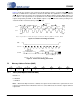
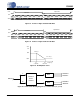
7.4.1 Writing in SPI
Figure 8 shows the operation of the control port in SPI format. To write to a register, bring CS low. The
first 7 bits on CDIN form the chip address and must be 0011000. The eighth bit is a read/write indicator
(R/W
), which must be low to write. The next 8 bits form the Memory Address Pointer (MAP), which is set
to the address of the register that is to be updated. The next 8 bits are the data which will be placed into
register designated by the MAP. To write multiple registers, keep CS
low and continue providing clocks
on CCLK. End the read transaction by setting CS
high.
7.5 Memory Address Pointer (MAP)
7.5.1 INCR (Auto Map Increment Enable)
Default = ‘0’
0 - Disabled
1 - Enabled
Note: When Auto Map Increment is enabled, the register must be written it two separate blocks: from
register 01h to 08h and then from 09h and 11h. The counter will not auto-increment to register 09h from
register 08h
76543210
INCR Reserved Reserved MAP4 MAP3 MAP2 MAP1 MAP0
00000000
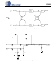
SDA
SCL
001100
ADDR
AD0
R/W
Start
ACK
DATA
1-8
ACK
DATA
1-8
ACK
Stop
Note: If operation is a write, this byte contains the Memory Address Pointer, MAP.
Note 1
Figure 7. Control Port Timing, I²C Format
MAP
MSB
LSB
DATA
byte 1
byte n
R/W
MAP = Memory Address Pointer
ADDRESS
CHIP
CDIN
CCLK
CS
0011000
Figure 8. Control Port Timing, SPI Format