
Manual

DS514F2 25
CS4382
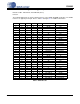
5. PIN DESCRIPTION
Pin Name # Pin Description
VD 4
Digital Power (Input) - Positive power supply for the digital section. Refer to the Recommended Operat-
ing Conditions for appropriate voltages.
GND
5
31
Ground (Input) - Ground reference. Should be connected to analog ground.
MCLK 6
Master Clock (Input) - Clock source for the delta-sigma modulator and digital filters. Table 5 illustrates
several standard audio sample rates and the required master clock frequency.
LRCK1
LRCK2
7
10
Left Right Clock (Input) - Determines which channel, Left or Right, is currently active on the serial audio
data line. The frequency of the left/right clock must be at the audio sample rate, Fs.
SDIN1
SDIN2
SDIN3
SDIN4
8
11
13
14
Serial Audio Data Input (Input) - Input for two’s complement serial audio data.
SCLK1
SCLK2
9
12
Serial Clock (Input) - Serial clock for the serial audio interface.
VLC 18
Control Port Power (Input) - Determines the required signal level for the control port. Refer to the Rec-
ommended Operating Conditions for appropriate voltages.
RST
19
Reset (Input) - The device enters a low power mode and all internal registers are reset to their default
settings when low.
FILT+ 20
Positive Voltage Reference (Output) - Positive reference voltage for the internal sampling circuits.
Requires the capacitive decoupling to analog ground, as shown in the Typical Connection Diagram.
VQ 21
Quiescent Voltage (Output) - Filter connection for internal quiescent voltage. VQ must be capacitively
coupled to analog ground, as shown in the Typical Connection Diagram. The nominal voltage level is
specified in the Analog Characteristics and Specifications section. VQ presents an appreciable source
impedance and any current drawn from this pin will alter device performance.
However, VQ can be used to bias the analog circuitry assuming there is no AC signal component and
the DC current is less than the maximum specified in the Analog Characteristics and Specifications sec-
tion.
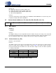
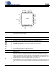
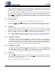
SDIN3
GND
AOUTB2-
AOUTA3+
AOUTB3-
AOUTB2+
VA
AOUTA3-
AOUTB3+
6
2
4
8
10
1
3
5
7
9
11
12
13 14 15 16 17 18 19 20 21 22 23 24
31
35
33
29
27
36
34
32
30
28
26
25
48 47 46 45 44 43 42 41 40 39 38 37
MCLK
DSDB1
VD
SDIN1
LRCK2
DSDA2
DSDA1
GND
SCLK1
SDIN2
SCLK2
LRCK1(DSD_EN)
M3(DSD_SCLK)
DSDB3
DSDA3
DSDA4
CS4382
DSDB4
VLS
SDIN4
M2(SCL/CCLK)
M1(SDA/CDIN)
VLC
RST
FILT+
VQ
MUTEC234
M0(AD0/CS)
AOUTA2+
AOUTA2-
AOUTB1+
AOUTB1-
AOUTA1-
AOUTA1+
DSDB2
MUTEC1
AOUTA4-
AOUTA4+
AOUTB4+
AOUTB4-