
Manual
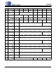

14 DS514F2
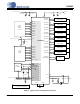
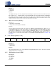
CS4382
Digital
Audio
Source
VLS
CS4382
MCLK
VD
AOUTA1+
10
8
32
0.1 µF
+
1 µF
+3.3 V to +5 V
SDIN1
9
1 µF
0.1 µ
F
+
+
20
21
FILT+
VQ
7
6
LRCK1
SCLK1
SDIN3
SDIN2
39
40
0.1 µ
F
47 µF
VA
0.1 µF
+
1 µF
0.1 µF
+1.8 V to +5 V
+5 V
4
43
SDIN4
LRCK2
SCLK2
13
14
Analog Conditioning
and Muting
AOUTA1-
AOUTB1+
38
37
Analog Conditioning
and Muting
AOUTB1-
AOUTA2+
35
36
Analog Conditioning
and Muting
AOUTA2-
AOUTB2+
34
33
Analog Conditioning
and Muting
AOUTB2-
AOUTA3+
29
30
Analog Conditioning
and Muting
AOUTA3-
AOUTB3+
28
27
Analog Conditioning
and Muting
AOUTB3-
AOUTA4+
25
26
Analog Conditioning
and Muting
AOUTA4-
AOUTB4+
24
23
Analog Conditioning
and Muting
AOUTB4-
MUTEC234
22
41
Mute
Drive
MUTEC1
11
12
PCM
31
GND
GND
5
Stand-Alone
Mode
Configuration
VLC
0.1 µF
+1.8 V to +5 V
18
DSD
Audio
Source
2
48
DSDB2
3
42
M3(DSD_SCLK)
DSDA1
DSDB3
DSDA3
DSDA4
DSDB1
DSDA2
46
45
47
1
44
DSDB4
16
15
M2
M1
M0
RST
19
17
47 K
Ω
VLS
Note
DSD
Note
DSD
: For DSD operation:
1) LRCK1 must be tied to VLS and
remain static high.
2) M3 PCM stand-alone configuration
pin becomes DSD_SCLK
Mute
Drive
47 K
Ω
Note
DSD
Note
VLC
Note
VLC
: If series resistors are
used they must be <1 kOhm. If
possible tie VLC to the VD supply
to reduce possible excess current
consumption from VLC.
Figure 6. Typical Connection Diagram Stand-Alone