
Manual

CS4373A
DS699F2 31
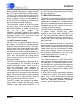
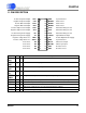
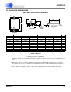
11. PIN DESCRIPTION
1
2
3
4
5
6
7
821
22
23
24
25
26
27
28
9
10
11
12 17
18
19
20
13
14 15
16
Positive Capacitor Output CAP+
Negative Capacitor Output CAP-
Positive Buffered Output BUF+
Negative Buffered Output BUF-
Positive High Precision Output OUT+
Negative High Precision Output OUT-
Positive Analog Power Supply VA+
Negative Analog Power Supply VA-
Negative Voltage Reference VREF-
Positive Voltage Reference VREF+
No Connect NC
No Connect NC
No Connect NC
No Connect NC
GND System Ground
MODE0 Mode Select
MODE1 Mode Select
MODE2 Mode Select
ATT0 Attenuation Range Select
ATT1 Attenuation Range Select
ATT2 Attenuation Range Select
TDATA Signal Bitstream Input
VD Positive Digital Power Supply
GND System Ground
MCLK Master Clock Input
MSYNC Master Sync Input
DNC Do Not Connect
DNC Do Not Connect
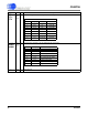
Pin Name Pin # I/O
Pin Description
CAP+,
CAP-
1
2
O
Capacitor connection for internal anti-alias filter.
BUF+,
BUF-
3
4
O
Buffered differential analog output.
OUT+,
OUT-
5
6
O
Precision differential analog output.
VA+,
VA-
7
8
I
Analog power supply. Refer to the Specified Operating Conditions.
VREF-,
VREF+
9
10
I Voltage reference input. Refer to the Specified Operating Conditions.
MSYNC
17 I
Master Sync Input. Low to high transition resets the internal clock phasing.
MCLK
18
I Master Clock Input. CMOS compatible clock input.
GND
19
System ground.
VD
20
Digital power supply. Refer to the Specified Operating Conditions.
TDATA
21 I
Test Bit Stream input from digital filter TBS generator.