
Manual

CS4373A
24 DS699F2
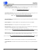
7. ANALOG OUTPUTS
The CS4373A has multiple differential analog
outputs. The best possible analog perfor-
mance is achieved from the precision outputs
(OUT±), but with only minimal drive capability.
A buffered output (BUF±) can drive an external
load, but with reduced analog performance.
The internal anti-alias filter requires a dedicat-
ed capacitor connection (CAP±) to eliminate
undesired high-frequency signals.
7.1 Differential Signals
Differential AC signals out of the CS4373A
consist of two halves with equal but opposite
magnitude varying about a common mode
voltage. A full-scale 5 V
PP
differential AC sig-
nal centered on a -0.15 V common mode volt-
age will have:
SIG+ = -0.15 V + 1.25 V = +1.1 V
SIG- = -0.15 V - 1.25 V = -1.4 V
SIG+ is +2.5 V relative to SIG-
For the opposite case:
SIG+ = -0.15 V - 1.25 V = -1.4 V
SIG- = -0.15 V + 1.25 V = +1.1 V
SIG+ is -2.5 V relative to SIG-
So the total swing for SIG+ relative to SIG- is
(+2.5 V) - (-2.5 V) = 5 V
pp
differential. A similar
calculation can be done for SIG- relative to
SIG+. It’s important to note that a 5 V
pp
differ-
ential signal centered on a -0.15 V common
mode voltage never exceeds +1.1 V with re-
spect to ground and never drops below -1.4 V
with respect to ground on either half. By defini-
tion, differential voltages are measured with
respect to the opposite half, not relative to
ground. A voltmeter differentially measuring
between SIG+ and SIG- in the above example
would read 1.767 V
rms
, or 5 V
pp
.
7.2 Analog Output Attenuation
The CS4373A has seven analog output atten-
uation settings from 1/1 to 1/64 selected with
the ATT2, ATT1, and ATT0 pins. At 1/64 atten-
uation in AC Common Mode (MODE 6) there
is no output signal amplitude due to the atten-
uator architecture.
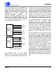
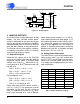
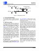
CS4373A
TDATA
CAP+
CAP-
BUF+
BUF-
OUT+
OUT-
MCLK
MSYNC
DGND
MODE1
MODE2
ATT0
ATT1
MODE0
ATT2
VA-
2.5 V
VREF
10 Ω
VREF+
VREF-
100µF
VA+
VA- VD
0.1µF 0.1µF
VDVA+
10nF
C0G
Analog
Switches
CH1 BUF
CH2 BUF
CH3 BUF
CH4 BUF
CH1,2,3,4 OUT
SWITCH
CONTROL
GPIO
CS5376A
SIGNALS
MCLK
MSYNC
TBSDATA
GPIO
GPIO
GPIO
GPIO
GPIO
ELECTRONICS
SENSOR
VA-
0.1µF
VA-
+
Route VREF as diff pair
Route OUT as diff pair
Route BUF as diff pair
Figure 12. Analog Outputs
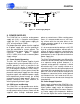
Table 3. Output Attenuation Settings
Selection ATT[2:0] Attenuation dB
0 0 0 0 1/1 0 dB
1 0 0 1 1/2 -6.02 dB
2 010 1/4 -12.04dB
3011 1/8-18.06dB
4 1 0 0 1/16 -24.08 dB
5 1 0 1 1/32 -30.10 dB
6 1 1 0 1/64 -36.12 dB
7 1 1 1 reserved reserved