
Manual

CS4373A
12 DS699F2
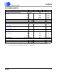
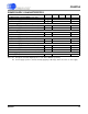
DIGITAL CHARACTERISTICS
Notes: 22. Device is intended to be driven with CMOS logic levels.
23. TDATA is generated by the test bit stream generator in the CS5376A digital filter.
24. TBSGAIN register value in the CS5376A digital filter.
Parameter Symbol Min Typ Max Unit
Digital Inputs
High-level Input Drive Voltage (Note 22)V
IH
0.6*VD - VD V
Low-level Input Drive Voltage (Note 22)V
IL
0.0 - 0.8 V
Input Leakage Current I
IN
-+1+10 µA
Digital Input Capacitance (Note 8) C
IN
-9- pF
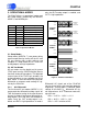
Rise Times Except MCLK (Note 8) t
RISE
--100ns
Fall Times Except MCLK (Note 8) t
FALL
--100ns
TDATA Input
TDATA Input Bit Rate (Note 23)f
tdata
- 256 - kbits/s
TDATA Input One’s Density Range (Note 8)INR
OD
25 - 75 %
TBSGAIN Full-scale Code (Note 24)TBS
FS
-
0x04B8F2
-
TBSGAIN -20 dB Code (Note 24)TBS
-20dB
-
0x0078E5
-
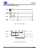
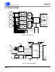
0.9 * VD
0.1 * VD
t
fall
t
rise
Figure 1. Digital Input Rise and Fall Times