
User Manual


Table Of Contents
- 1. Pin Description
- 2. Characteristics and Specifications
- Recommended Operating Conditions
- Absolute Maximum Ratings
- DAC Analog Characteristics
- Power and Thermal Characteristics
- Combined Interpolation & On-Chip Analog Filter Response
- Combined Interpolation & On-Chip Analog Filter Response
- DSD Combined Digital & On-Chip Analog Filter Response
- Digital Characteristics
- Switching Characteristics - PCM
- Switching Characteristics - DSD
- Switching Characteristics - Control Port - I·C Format
- Switching Characteristics - Control Port - SPI Format
- 3. Typical Connection Diagram
- 4. Applications
- 4.1 Master Clock
- 4.2 Mode Select
- 4.3 Digital Interface Formats
- Figure 8. Format 0 - Left-Justified up to 24-bit Data
- Figure 9. Format 1 - I·S up to 24-bit Data
- Figure 10. Format 2 - Right-Justified 16-bit Data
- Figure 11. Format 3 - Right-Justified 24-bit Data
- Figure 12. Format 4 - Right-Justified 20-bit Data
- Figure 13. Format 5 - Right-Justified 18-bit Data
- 4.3.1 OLM #1
- 4.3.2 OLM #2
- 4.4 Oversampling Modes
- 4.5 Interpolation Filter
- 4.6 De-Emphasis
- 4.7 ATAPI Specification
- 4.8 Direct Stream Digital (DSD) Mode
- 4.9 Grounding and Power Supply Arrangements
- 4.10 Analog Output and Filtering
- 4.11 The MUTEC Outputs
- 4.12 Recommended Power-Up Sequence
- 4.13 Recommended Procedure for Switching Operational Modes
- 4.14 Control Port Interface
- 4.15 Memory Address Pointer (MAP)
- 5. Register Quick Reference
- 6. Register Description
- 6.1 Chip Revision (Address 01h)
- 6.2 Mode Control 1 (Address 02h)
- 6.3 PCM Control (Address 03h)
- 6.4 DSD Control (Address 04h)
- 6.5 Filter Control (Address 05h)
- 6.6 Invert Control (Address 06h)
- 6.7 Group Control (Address 07h)
- 6.8 Ramp and Mute (Address 08h)
- 6.9 Mute Control (Address 09h)
- 6.10 Mixing Control (Address 0Ah, 0Dh, 10h, 13h)
- 6.11 Volume Control (Address 0Bh, 0Ch, 0Eh, 0Fh, 11h, 12h)
- 6.12 PCM Clock Mode (Address 16h)
- 7. Filter Response Plots
- Figure 24. Single-Speed (fast) Stopband Rejection
- Figure 25. Single-Speed (fast) Transition Band
- Figure 26. Single-Speed (fast) Transition Band (detail)
- Figure 27. Single-Speed (fast) Passband Ripple
- Figure 28. Single-Speed (slow) Stopband Rejection
- Figure 29. Single-Speed (slow) Transition Band
- Figure 30. Single-Speed (slow) Transition Band (detail)
- Figure 31. Single-Speed (slow) Passband Ripple
- Figure 32. Double-Speed (fast) Stopband Rejection
- Figure 33. Double-Speed (fast) Transition Band
- Figure 34. Double-Speed (fast) Transition Band (detail)
- Figure 35. Double-Speed (fast) Passband Ripple
- Figure 36. Double-Speed (slow) Stopband Rejection
- Figure 37. Double-Speed (slow) Transition Band
- Figure 38. Double-Speed (slow) Transition Band (detail)
- Figure 39. Double-Speed (slow) Passband Ripple
- Figure 40. Quad-Speed (fast) Stopband Rejection
- Figure 41. Quad-Speed (fast) Transition Band
- Figure 42. Quad-Speed (fast) Transition Band (detail)
- Figure 43. Quad-Speed (fast) Passband Ripple
- Figure 44. Quad-Speed (slow) Stopband Rejection
- Figure 45. Quad-Speed (slow) Transition Band
- Figure 46. Quad-Speed (slow) Transition Band (detail)
- Figure 47. Quad-Speed (slow) Passband Ripple
- 8. References
- 9. Parameter Definitions
- 10. Package Dimensions
- 11. Ordering Information
- 12. Revision History
6 DS619F1
CS4364
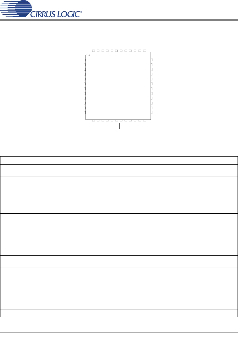
1. PIN DESCRIPTION
Pin Name # Pin Description
VD 4
Digital Power (Input) - Positive power supply for the digital section. Refer to the Recommended
Operating Conditions for appropriate voltages.
GND
5
31
Ground (Input) - Ground reference. Should be connected to analog ground.
MCLK 6
Master Clock (Input) - Clock source for the delta-sigma modulator and digital filters. Table 1 illus-
trates several standard audio sample rates and the required master clock frequencies.
LRCK 7
Left Right Clock (Input) - Determines which channel, Left or Right, is currently active on the
serial audio data line. The frequency of the left/right clock must be at the audio sample rate, Fs.
SDIN1
SDIN2
SDIN3
8
11
13
Serial Data Input (Input) - Input for two’s complement serial audio data.
SCLK 9 Serial Clock (Input) - Serial clocks for the serial audio interface.
TST
14
44
45
Test - These pins need to be tied to analog ground.
RST
19
Reset (Input) - The device enters a low power mode and all internal registers are reset to their
default settings when low.
VA 32
Analog Power (Input) - Positive power supply for the analog section. Refer to the Recommended
Operating Conditions for appropriate voltages.
VLS 43
Serial Audio Interface Power (Input) - Determines the required signal level for the serial audio
interface. Refer to the Recommended Operating Conditions for appropriate voltages.
VLC 18
Control Port Power (Input) - Determines the required signal level for the control port and hard-
ware mode configuration pins. Refer to the Recommended Operating Conditions for appropriate
voltages.
VQ 21 Quiescent Voltage (Output) - Filter connection for internal quiescent voltage.
SDIN3
GND
TST_OUT
AOUT5
TST_OUT
AOUT4
VA
TST_OUT
AOUT6
MUTE2
MUTE3
6
2
4
8
10
1
3
5
7
9
11
1
2
13 14 15 16 17 18 19 20 21 22
23 24
31
35
33
29
27
36
34
32
30
28
26
25
48 47 46 45 44 43 42 41 40 39 38 37
MCLK
DSD2
VD
SDIN1
M4(TST)
DSD3
DSD1
GND
SCLK
SDIN2
M3(TST)
LRCK
DSD_SCLK
DSD6
DSD5
TST
CS4364
TST
VLS
TST
M2(SCL/CCLK)
M1(SDA/CDIN)
VLC
RST
FILT+
VQ
MUTE6
MUTE5
MUTE4
M0(AD0/CS)
AOUT3
TST_OUT
AOUT2
TST_OUT
TST_OUT
AOUT1
DSD4
MUTE1