
User Manual


Table Of Contents
- 1. Pin Description
- 2. Characteristics and Specifications
- Recommended Operating Conditions
- Absolute Maximum Ratings
- DAC Analog Characteristics
- Power and Thermal Characteristics
- Combined Interpolation & On-Chip Analog Filter Response
- Combined Interpolation & On-Chip Analog Filter Response
- DSD Combined Digital & On-Chip Analog Filter Response
- Digital Characteristics
- Switching Characteristics - PCM
- Switching Characteristics - DSD
- Switching Characteristics - Control Port - I·C Format
- Switching Characteristics - Control Port - SPI Format
- 3. Typical Connection Diagram
- 4. Applications
- 4.1 Master Clock
- 4.2 Mode Select
- 4.3 Digital Interface Formats
- Figure 8. Format 0 - Left-Justified up to 24-bit Data
- Figure 9. Format 1 - I·S up to 24-bit Data
- Figure 10. Format 2 - Right-Justified 16-bit Data
- Figure 11. Format 3 - Right-Justified 24-bit Data
- Figure 12. Format 4 - Right-Justified 20-bit Data
- Figure 13. Format 5 - Right-Justified 18-bit Data
- 4.3.1 OLM #1
- 4.3.2 OLM #2
- 4.4 Oversampling Modes
- 4.5 Interpolation Filter
- 4.6 De-Emphasis
- 4.7 ATAPI Specification
- 4.8 Direct Stream Digital (DSD) Mode
- 4.9 Grounding and Power Supply Arrangements
- 4.10 Analog Output and Filtering
- 4.11 The MUTEC Outputs
- 4.12 Recommended Power-Up Sequence
- 4.13 Recommended Procedure for Switching Operational Modes
- 4.14 Control Port Interface
- 4.15 Memory Address Pointer (MAP)
- 5. Register Quick Reference
- 6. Register Description
- 6.1 Chip Revision (Address 01h)
- 6.2 Mode Control 1 (Address 02h)
- 6.3 PCM Control (Address 03h)
- 6.4 DSD Control (Address 04h)
- 6.5 Filter Control (Address 05h)
- 6.6 Invert Control (Address 06h)
- 6.7 Group Control (Address 07h)
- 6.8 Ramp and Mute (Address 08h)
- 6.9 Mute Control (Address 09h)
- 6.10 Mixing Control (Address 0Ah, 0Dh, 10h, 13h)
- 6.11 Volume Control (Address 0Bh, 0Ch, 0Eh, 0Fh, 11h, 12h)
- 6.12 PCM Clock Mode (Address 16h)
- 7. Filter Response Plots
- Figure 24. Single-Speed (fast) Stopband Rejection
- Figure 25. Single-Speed (fast) Transition Band
- Figure 26. Single-Speed (fast) Transition Band (detail)
- Figure 27. Single-Speed (fast) Passband Ripple
- Figure 28. Single-Speed (slow) Stopband Rejection
- Figure 29. Single-Speed (slow) Transition Band
- Figure 30. Single-Speed (slow) Transition Band (detail)
- Figure 31. Single-Speed (slow) Passband Ripple
- Figure 32. Double-Speed (fast) Stopband Rejection
- Figure 33. Double-Speed (fast) Transition Band
- Figure 34. Double-Speed (fast) Transition Band (detail)
- Figure 35. Double-Speed (fast) Passband Ripple
- Figure 36. Double-Speed (slow) Stopband Rejection
- Figure 37. Double-Speed (slow) Transition Band
- Figure 38. Double-Speed (slow) Transition Band (detail)
- Figure 39. Double-Speed (slow) Passband Ripple
- Figure 40. Quad-Speed (fast) Stopband Rejection
- Figure 41. Quad-Speed (fast) Transition Band
- Figure 42. Quad-Speed (fast) Transition Band (detail)
- Figure 43. Quad-Speed (fast) Passband Ripple
- Figure 44. Quad-Speed (slow) Stopband Rejection
- Figure 45. Quad-Speed (slow) Transition Band
- Figure 46. Quad-Speed (slow) Transition Band (detail)
- Figure 47. Quad-Speed (slow) Passband Ripple
- 8. References
- 9. Parameter Definitions
- 10. Package Dimensions
- 11. Ordering Information
- 12. Revision History
DS619F1 37
CS4364
6.5 Filter Control (Address 05h)
6.5.1 Interpolation Filter Select (FILT_SEL)
Function:
When set to 0 (default), the Interpolation Filter has a fast roll off.
When set to 1, the Interpolation Filter has a slow roll off.
The specifications for each filter can be found in the Analog characteristics table, and response plots can
be found in Figures 22 to 45.
6.6 Invert Control (Address 06h)
6.6.1 Invert Signal Polarity (INV_xx)
Function:
When set to 1, this bit inverts the signal polarity of channel xx.
When set to 0 (default), this function is disabled.
6.7 Group Control (Address 07h)
6.7.1 Mute Pin Control (MUTEC1, MUTEC0)
Default = 00
00 - Six mute control signals
01, 10 - One mute control signal
11 - Three mute control signals
Function:
Selects how the internal mute control signals are routed to the MUTEC1 through MUTEC6 pins. When
set to ‘00’, there is one mute control signal for each channel: AOUT1A on MUTEC1, AOUT1B on
MUTEC2, etc. When set to ‘01’ or ‘10’, there is a single mute control signal on the MUTEC1 pin. When
set to ‘11’, there are three mute control signals, one for each stereo pair: AOUT1A and AOUT1B on
MUTEC1, AOUT2A and AOUT2B on MUTEC2, and AOUT3A and AOUT3B on MUTEC3.
6.7.2 Channel A Volume = Channel B Volume (Px_A=B)
Default = 0
0 - Disabled
1 - Enabled
76543210
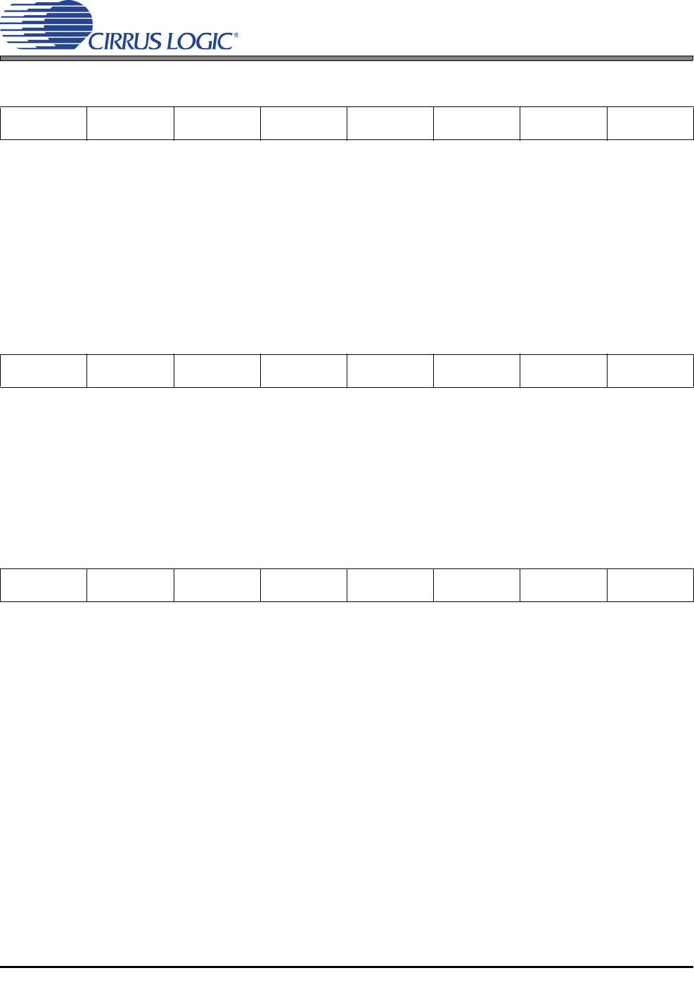
Reserved Reserved Reserved Reserved Reserved Reserved Reserved FILT_SEL
00000000
76543210
Reserved Reserved INV_B3 INV_A3 INV_B2 INV_A2 INV_B1 INV_A1
00000000
76543210
MUTEC1 MUTEC0 Reserved P1_A=B P2_A=B P3_A=B Reserved SNGLVOL
00000000