
User Manual


Table Of Contents
- 1. Pin Description
- 2. Characteristics and Specifications
- Recommended Operating Conditions
- Absolute Maximum Ratings
- DAC Analog Characteristics
- Power and Thermal Characteristics
- Combined Interpolation & On-Chip Analog Filter Response
- Combined Interpolation & On-Chip Analog Filter Response
- DSD Combined Digital & On-Chip Analog Filter Response
- Digital Characteristics
- Switching Characteristics - PCM
- Switching Characteristics - DSD
- Switching Characteristics - Control Port - I·C Format
- Switching Characteristics - Control Port - SPI Format
- 3. Typical Connection Diagram
- 4. Applications
- 4.1 Master Clock
- 4.2 Mode Select
- 4.3 Digital Interface Formats
- Figure 8. Format 0 - Left-Justified up to 24-bit Data
- Figure 9. Format 1 - I·S up to 24-bit Data
- Figure 10. Format 2 - Right-Justified 16-bit Data
- Figure 11. Format 3 - Right-Justified 24-bit Data
- Figure 12. Format 4 - Right-Justified 20-bit Data
- Figure 13. Format 5 - Right-Justified 18-bit Data
- 4.3.1 OLM #1
- 4.3.2 OLM #2
- 4.4 Oversampling Modes
- 4.5 Interpolation Filter
- 4.6 De-Emphasis
- 4.7 ATAPI Specification
- 4.8 Direct Stream Digital (DSD) Mode
- 4.9 Grounding and Power Supply Arrangements
- 4.10 Analog Output and Filtering
- 4.11 The MUTEC Outputs
- 4.12 Recommended Power-Up Sequence
- 4.13 Recommended Procedure for Switching Operational Modes
- 4.14 Control Port Interface
- 4.15 Memory Address Pointer (MAP)
- 5. Register Quick Reference
- 6. Register Description
- 6.1 Chip Revision (Address 01h)
- 6.2 Mode Control 1 (Address 02h)
- 6.3 PCM Control (Address 03h)
- 6.4 DSD Control (Address 04h)
- 6.5 Filter Control (Address 05h)
- 6.6 Invert Control (Address 06h)
- 6.7 Group Control (Address 07h)
- 6.8 Ramp and Mute (Address 08h)
- 6.9 Mute Control (Address 09h)
- 6.10 Mixing Control (Address 0Ah, 0Dh, 10h, 13h)
- 6.11 Volume Control (Address 0Bh, 0Ch, 0Eh, 0Fh, 11h, 12h)
- 6.12 PCM Clock Mode (Address 16h)
- 7. Filter Response Plots
- Figure 24. Single-Speed (fast) Stopband Rejection
- Figure 25. Single-Speed (fast) Transition Band
- Figure 26. Single-Speed (fast) Transition Band (detail)
- Figure 27. Single-Speed (fast) Passband Ripple
- Figure 28. Single-Speed (slow) Stopband Rejection
- Figure 29. Single-Speed (slow) Transition Band
- Figure 30. Single-Speed (slow) Transition Band (detail)
- Figure 31. Single-Speed (slow) Passband Ripple
- Figure 32. Double-Speed (fast) Stopband Rejection
- Figure 33. Double-Speed (fast) Transition Band
- Figure 34. Double-Speed (fast) Transition Band (detail)
- Figure 35. Double-Speed (fast) Passband Ripple
- Figure 36. Double-Speed (slow) Stopband Rejection
- Figure 37. Double-Speed (slow) Transition Band
- Figure 38. Double-Speed (slow) Transition Band (detail)
- Figure 39. Double-Speed (slow) Passband Ripple
- Figure 40. Quad-Speed (fast) Stopband Rejection
- Figure 41. Quad-Speed (fast) Transition Band
- Figure 42. Quad-Speed (fast) Transition Band (detail)
- Figure 43. Quad-Speed (fast) Passband Ripple
- Figure 44. Quad-Speed (slow) Stopband Rejection
- Figure 45. Quad-Speed (slow) Transition Band
- Figure 46. Quad-Speed (slow) Transition Band (detail)
- Figure 47. Quad-Speed (slow) Passband Ripple
- 8. References
- 9. Parameter Definitions
- 10. Package Dimensions
- 11. Ordering Information
- 12. Revision History
32 DS619F1
CS4364
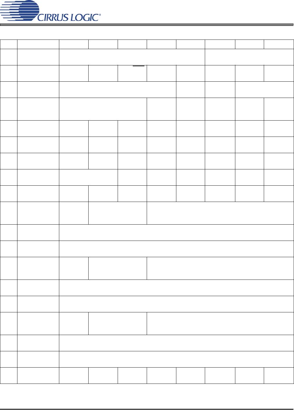
5. REGISTER QUICK REFERENCE
Addr Function 7 6 5 4 3 2 1 0
01h Chip Revision PART4 PART3 PART2 PART1 PART0 REV2 REV1 REV0
default 0 1 1 0 0 x x x
02h Mode Control CPEN FREEZE DSD/PCM
Reserved DAC3_DIS DAC2_DIS DAC1_DIS PDN
default00000001
03h PCM Control DIF3 DIF2 DIF1 DIF0 Reserved Reserved FM1 FM0
default00000011
04h DSD Control DSD_DIF2 DSD_DIF1 DSD_DIF0 DIR_DSD STATIC_D
SD
INVALID_D
SD
DSD_PM_
MD
DSD_PM_
EN
default00001000
05h Filter Control Reserved Reserved Reserved Reserved Reserved Reserved Reserved FILT_SEL
default00000000
06h Invert Control Reserved Reserved INV_B3 INV_A3 INV_B2 INV_A2 INV_B1 INV_A1
default00000000
07h Group Control MUTEC1 MUTEC0 Reserved P1_A=B P2_A=B P3_A=B Reserved SNGLVOL
default00000000
08h Ramp and Mute SZC1 SZC0 RMP_UP RMP_DN PAMUTE DAMUTE MUTE_P1 MUTE_P0
default10111100
09h Mute Control Reserved Reserved MUTE_B3 MUTE_A3 MUTE_B2 MUTE_A2 MUTE_B1 MUTE_A1
default00000000
0Ah Mixing Control
Pair 1 (AOUTx1)
Reserved P1_DEM1 P1_DEM0 P1ATAPI4 P1ATAPI3 P1ATAPI2 P1ATAPI1 P1ATAPI0
default00001001
0Bh Vol. Control A1 A1_VOL7 A1_VOL6 A1_VOL5 A1_VOL4 A1_VOL3 A1_VOL2 A1_VOL1 A1_VOL0
default00000000
0Ch Vol. Control B1 B1_VOL7 B1_VOL6 B1_VOL5 B1_VOL4 B1_VOL3 B1_VOL2 B1_VOL1 B1_VOL0
default00000000
0Dh Mixing Control
Pair 2 (AOUTx1)
Reserved P2_DEM1 P2_DEM0 P2ATAPI4 P2ATAPI3 P2ATAPI2 P2ATAPI1 P2ATAPI0
default00001001
0Eh Vol. Control A2 A2_VOL7 A2_VOL6 A2_VOL5 A2_VOL4 A2_VOL3 A2_VOL2 A2_VOL1 A2_VOL0
default00000000
0Fh Vol. Control B2 B2_VOL7 B2_VOL6 B2_VOL5 B2_VOL4 B2_VOL3 B2_VOL2 B2_VOL1 B2_VOL0
default00000000
10h Mixing Control
Pair 3 (AOUTx1)
Reserved P3_DEM1 P3_DEM0 P3ATAPI4 P3ATAPI3 P3ATAPI2 P3ATAPI1 P3ATAPI0
default00001001
11h Vol. Control A3 A3_VOL7 A3_VOL6 A3_VOL5 A3_VOL4 A3_VOL3 A3_VOL2 A3_VOL1 A3_VOL0
default00000000
12h Vol. Control B3 B3_VOL7 B3_VOL6 B3_VOL5 B3_VOL4 B3_VOL3 B3_VOL2 B3_VOL1 B3_VOL0
default00000000
16h PCM clock mode Reserved Reserved MCLKDIV Reserved Reserved Reserved Reserved Reserved
default00000000