
User Manual


Table Of Contents
- 1. Pin Description
- 2. Characteristics and Specifications
- Recommended Operating Conditions
- Absolute Maximum Ratings
- DAC Analog Characteristics
- Power and Thermal Characteristics
- Combined Interpolation & On-Chip Analog Filter Response
- Combined Interpolation & On-Chip Analog Filter Response
- DSD Combined Digital & On-Chip Analog Filter Response
- Digital Characteristics
- Switching Characteristics - PCM
- Switching Characteristics - DSD
- Switching Characteristics - Control Port - I·C Format
- Switching Characteristics - Control Port - SPI Format
- 3. Typical Connection Diagram
- 4. Applications
- 4.1 Master Clock
- 4.2 Mode Select
- 4.3 Digital Interface Formats
- Figure 8. Format 0 - Left-Justified up to 24-bit Data
- Figure 9. Format 1 - I·S up to 24-bit Data
- Figure 10. Format 2 - Right-Justified 16-bit Data
- Figure 11. Format 3 - Right-Justified 24-bit Data
- Figure 12. Format 4 - Right-Justified 20-bit Data
- Figure 13. Format 5 - Right-Justified 18-bit Data
- 4.3.1 OLM #1
- 4.3.2 OLM #2
- 4.4 Oversampling Modes
- 4.5 Interpolation Filter
- 4.6 De-Emphasis
- 4.7 ATAPI Specification
- 4.8 Direct Stream Digital (DSD) Mode
- 4.9 Grounding and Power Supply Arrangements
- 4.10 Analog Output and Filtering
- 4.11 The MUTEC Outputs
- 4.12 Recommended Power-Up Sequence
- 4.13 Recommended Procedure for Switching Operational Modes
- 4.14 Control Port Interface
- 4.15 Memory Address Pointer (MAP)
- 5. Register Quick Reference
- 6. Register Description
- 6.1 Chip Revision (Address 01h)
- 6.2 Mode Control 1 (Address 02h)
- 6.3 PCM Control (Address 03h)
- 6.4 DSD Control (Address 04h)
- 6.5 Filter Control (Address 05h)
- 6.6 Invert Control (Address 06h)
- 6.7 Group Control (Address 07h)
- 6.8 Ramp and Mute (Address 08h)
- 6.9 Mute Control (Address 09h)
- 6.10 Mixing Control (Address 0Ah, 0Dh, 10h, 13h)
- 6.11 Volume Control (Address 0Bh, 0Ch, 0Eh, 0Fh, 11h, 12h)
- 6.12 PCM Clock Mode (Address 16h)
- 7. Filter Response Plots
- Figure 24. Single-Speed (fast) Stopband Rejection
- Figure 25. Single-Speed (fast) Transition Band
- Figure 26. Single-Speed (fast) Transition Band (detail)
- Figure 27. Single-Speed (fast) Passband Ripple
- Figure 28. Single-Speed (slow) Stopband Rejection
- Figure 29. Single-Speed (slow) Transition Band
- Figure 30. Single-Speed (slow) Transition Band (detail)
- Figure 31. Single-Speed (slow) Passband Ripple
- Figure 32. Double-Speed (fast) Stopband Rejection
- Figure 33. Double-Speed (fast) Transition Band
- Figure 34. Double-Speed (fast) Transition Band (detail)
- Figure 35. Double-Speed (fast) Passband Ripple
- Figure 36. Double-Speed (slow) Stopband Rejection
- Figure 37. Double-Speed (slow) Transition Band
- Figure 38. Double-Speed (slow) Transition Band (detail)
- Figure 39. Double-Speed (slow) Passband Ripple
- Figure 40. Quad-Speed (fast) Stopband Rejection
- Figure 41. Quad-Speed (fast) Transition Band
- Figure 42. Quad-Speed (fast) Transition Band (detail)
- Figure 43. Quad-Speed (fast) Passband Ripple
- Figure 44. Quad-Speed (slow) Stopband Rejection
- Figure 45. Quad-Speed (slow) Transition Band
- Figure 46. Quad-Speed (slow) Transition Band (detail)
- Figure 47. Quad-Speed (slow) Passband Ripple
- 8. References
- 9. Parameter Definitions
- 10. Package Dimensions
- 11. Ordering Information
- 12. Revision History
30 DS619F1
CS4364
4.14.2.2 I²C Read
To read from the device, follow the procedure below while adhering to the control port Switching Specifica-
tions.
1. Initiate a START condition to the
I²C bus followed by the address byte. The upper 6 bits must be
001100. The seventh bit must match the setting of the AD0 pin, and the eighth must be 1. The eighth
bit of the address byte is the R/W
bit.
2. After transmitting an acknowledge (ACK), the device will then transmit the contents of the register
pointed to by the MAP. The MAP register will contain the address of the last register written to the
MAP, or the default address (see Section 4.14.1) if an
I²C read is the first operation performed on the
device.
3. Once the device has transmitted the contents of the register pointed to by the MAP, issue an ACK.
4. If the INCR bit is set to 1, the device will continue to transmit the contents of successive registers. Con-
tinue providing a clock and issue an ACK after each byte until all the desired registers are read, then
initiate a STOP condition to the bus.
5. If the INCR bit is set to 0 and further
I²C reads from other registers are desired, it is necessary to initiate
a repeated START condition and follow the procedure detailed from steps 1 and 2 from the
I²C Write
instructions followed by step 1 of the
I²C Read section. If no further reads from other registers are de-
sired, initiate a STOP condition to the bus.
4.14.3 SPI Mode
In SPI Mode, data is clocked into the serial control data line, CDIN, by the serial control port clock, CCLK
(see Figure 23 for the clock to data relationship). There is no AD0 pin. Pin CS
is the chip select signal and
is used to control SPI writes to the control port. When the device detects a high to low transition on the
AD0/CS
pin after power-up, SPI Mode will be selected. All signals are inputs and data is clocked in on the
rising edge of CCLK.
4.14.3.1 SPI Write
To write to the device, follow the procedure below while adhering to the control port Switching Specifica-
tions in Section 2.
1. Bring CS
low.
2. The address byte on the CDIN pin must then be 00110000.
3. Write to the memory address pointer, MAP. This byte points to the register to be written.
4. Write the desired data to the register pointed to by the MAP.
5. If the INCR bit (see Section 4.14.1) is set to 1, repeat the previous step until all the desired registers
are written, then bring CS
high.
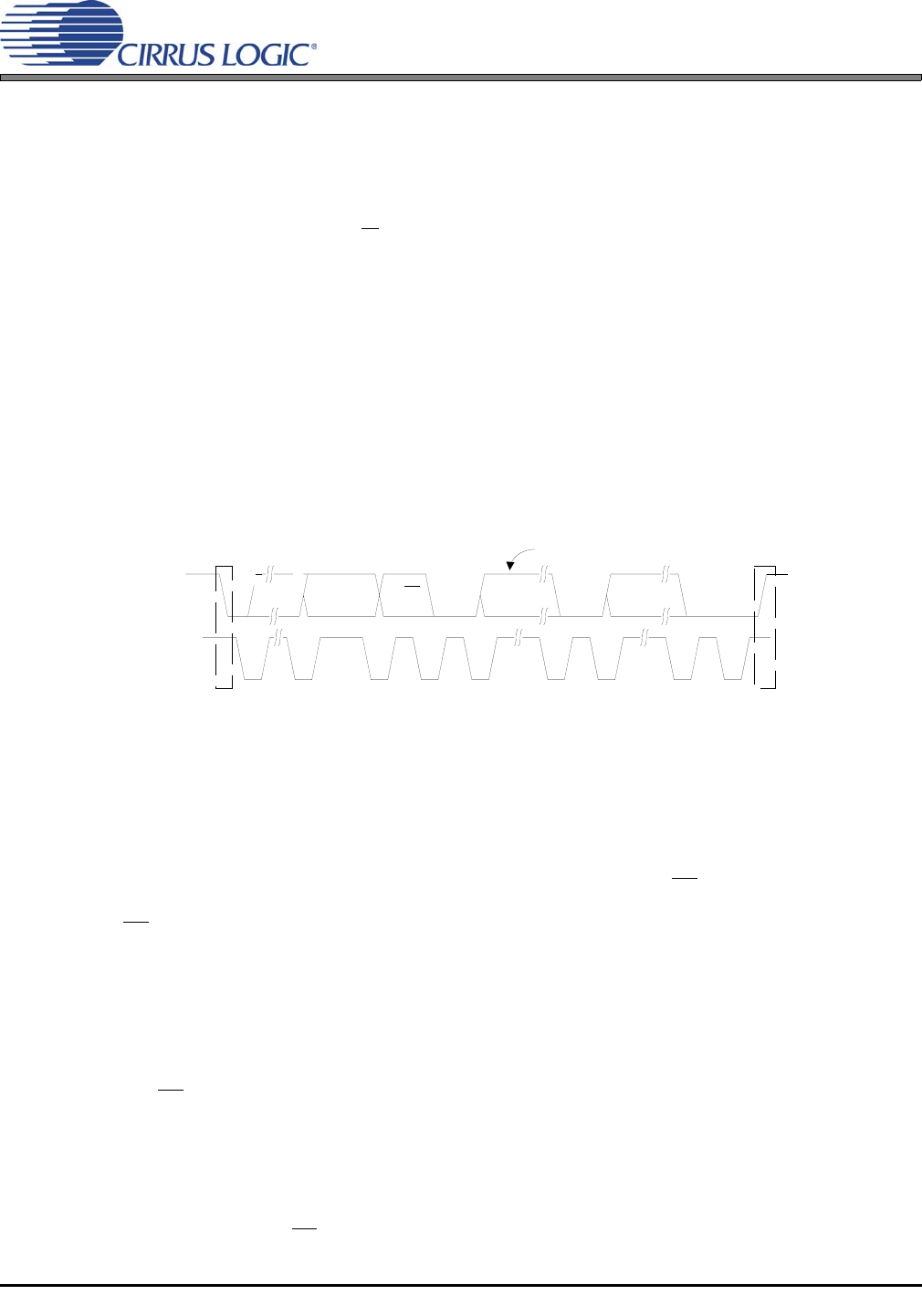
SDA
SCL
001100
ADDR
AD0
R/W
Start
ACK
DATA
1-8
ACK
DATA
1-8
ACK
Stop
Note: If operation is a write, this byte contains the Memory Address Pointer, MAP.
Note 1
Figure 22. Control Port Timing, I²C Mode