
User Manual


Table Of Contents
- 1. Pin Description
- 2. Characteristics and Specifications
- Recommended Operating Conditions
- Absolute Maximum Ratings
- DAC Analog Characteristics
- Power and Thermal Characteristics
- Combined Interpolation & On-Chip Analog Filter Response
- Combined Interpolation & On-Chip Analog Filter Response
- DSD Combined Digital & On-Chip Analog Filter Response
- Digital Characteristics
- Switching Characteristics - PCM
- Switching Characteristics - DSD
- Switching Characteristics - Control Port - I·C Format
- Switching Characteristics - Control Port - SPI Format
- 3. Typical Connection Diagram
- 4. Applications
- 4.1 Master Clock
- 4.2 Mode Select
- 4.3 Digital Interface Formats
- Figure 8. Format 0 - Left-Justified up to 24-bit Data
- Figure 9. Format 1 - I·S up to 24-bit Data
- Figure 10. Format 2 - Right-Justified 16-bit Data
- Figure 11. Format 3 - Right-Justified 24-bit Data
- Figure 12. Format 4 - Right-Justified 20-bit Data
- Figure 13. Format 5 - Right-Justified 18-bit Data
- 4.3.1 OLM #1
- 4.3.2 OLM #2
- 4.4 Oversampling Modes
- 4.5 Interpolation Filter
- 4.6 De-Emphasis
- 4.7 ATAPI Specification
- 4.8 Direct Stream Digital (DSD) Mode
- 4.9 Grounding and Power Supply Arrangements
- 4.10 Analog Output and Filtering
- 4.11 The MUTEC Outputs
- 4.12 Recommended Power-Up Sequence
- 4.13 Recommended Procedure for Switching Operational Modes
- 4.14 Control Port Interface
- 4.15 Memory Address Pointer (MAP)
- 5. Register Quick Reference
- 6. Register Description
- 6.1 Chip Revision (Address 01h)
- 6.2 Mode Control 1 (Address 02h)
- 6.3 PCM Control (Address 03h)
- 6.4 DSD Control (Address 04h)
- 6.5 Filter Control (Address 05h)
- 6.6 Invert Control (Address 06h)
- 6.7 Group Control (Address 07h)
- 6.8 Ramp and Mute (Address 08h)
- 6.9 Mute Control (Address 09h)
- 6.10 Mixing Control (Address 0Ah, 0Dh, 10h, 13h)
- 6.11 Volume Control (Address 0Bh, 0Ch, 0Eh, 0Fh, 11h, 12h)
- 6.12 PCM Clock Mode (Address 16h)
- 7. Filter Response Plots
- Figure 24. Single-Speed (fast) Stopband Rejection
- Figure 25. Single-Speed (fast) Transition Band
- Figure 26. Single-Speed (fast) Transition Band (detail)
- Figure 27. Single-Speed (fast) Passband Ripple
- Figure 28. Single-Speed (slow) Stopband Rejection
- Figure 29. Single-Speed (slow) Transition Band
- Figure 30. Single-Speed (slow) Transition Band (detail)
- Figure 31. Single-Speed (slow) Passband Ripple
- Figure 32. Double-Speed (fast) Stopband Rejection
- Figure 33. Double-Speed (fast) Transition Band
- Figure 34. Double-Speed (fast) Transition Band (detail)
- Figure 35. Double-Speed (fast) Passband Ripple
- Figure 36. Double-Speed (slow) Stopband Rejection
- Figure 37. Double-Speed (slow) Transition Band
- Figure 38. Double-Speed (slow) Transition Band (detail)
- Figure 39. Double-Speed (slow) Passband Ripple
- Figure 40. Quad-Speed (fast) Stopband Rejection
- Figure 41. Quad-Speed (fast) Transition Band
- Figure 42. Quad-Speed (fast) Transition Band (detail)
- Figure 43. Quad-Speed (fast) Passband Ripple
- Figure 44. Quad-Speed (slow) Stopband Rejection
- Figure 45. Quad-Speed (slow) Transition Band
- Figure 46. Quad-Speed (slow) Transition Band (detail)
- Figure 47. Quad-Speed (slow) Passband Ripple
- 8. References
- 9. Parameter Definitions
- 10. Package Dimensions
- 11. Ordering Information
- 12. Revision History
28 DS619F1
CS4364
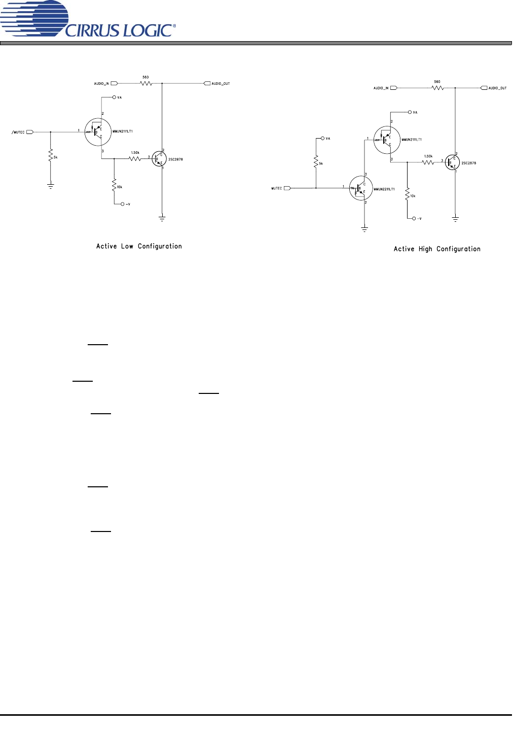
Figure 21. Recommended Mute Circuitry
4.12 Recommended Power-Up Sequence
4.12.1 Hardware Mode
1. Hold RST low until the power supplies and configuration pins are stable, and the master and left/right
clocks are locked to the appropriate frequencies, as discussed in Section 4.1. In this state, the
registers are reset to the default settings, FILT+ will remain low, and VQ will be connected to VA/2.
If RST
can not be held low long enough the SDINx pins should remain static low until all other clocks
are stable, and if possible the RST
should be toggled low again once the system is stable.
2. Bring RST
high. The device will remain in a low power state with FILT+ low and will initiate the
Hardware power-up sequence after approximately 512 LRCK cycles in Single-Speed Mode (1024
LRCK cycles in Double-Speed Mode, and 2048 LRCK cycles in Quad-Speed Mode).
4.12.2 Software Mode
1. Hold RST low until the power supply is stable, and the master and left/right clocks are locked to the
appropriate frequencies, as discussed in Section 4.1. In this state, the registers are reset to the default
settings, FILT+ will remain low, and VQ will be connected to VA/2.
2. Bring RST
high. The device will remain in a low power state with FILT+ low for 512 LRCK cycles in
Single-Speed Mode (1024 LRCK cycles in Double-Speed Mode, and 2048 LRCK cycles in Quad-
Speed Mode).
3. In order to reduce the chances of clicks and pops, perform a write to the CP_EN bit prior to the
completion of approximately 512 LRCK cycles in Single-Speed Mode (1024 LRCK cycles in Double-
Speed Mode, and 2048 LRCK cycles in Quad-Speed Mode). The desired register settings can be
loaded while keeping the PDN bit set to 1. Set the RMP_UP and RMP_DN bits to 1, then set the
format and mode control bits to the desired settings.
If more than the stated number of LRCK cycles passes before CPEN bit is written then the chip will
enter Hardware Mode and begin to operate with the M0-M4 as the mode settings. CPEN bit may be
written at anytime, even after the Hardware sequence has begun. It is advised that if the CPEN bit
can not be set in time then the SDINx pins should remain static low (this way no audio data can be