
User Manual


Table Of Contents
- 1. Pin Description
- 2. Characteristics and Specifications
- Recommended Operating Conditions
- Absolute Maximum Ratings
- DAC Analog Characteristics
- Power and Thermal Characteristics
- Combined Interpolation & On-Chip Analog Filter Response
- Combined Interpolation & On-Chip Analog Filter Response
- DSD Combined Digital & On-Chip Analog Filter Response
- Digital Characteristics
- Switching Characteristics - PCM
- Switching Characteristics - DSD
- Switching Characteristics - Control Port - I·C Format
- Switching Characteristics - Control Port - SPI Format
- 3. Typical Connection Diagram
- 4. Applications
- 4.1 Master Clock
- 4.2 Mode Select
- 4.3 Digital Interface Formats
- Figure 8. Format 0 - Left-Justified up to 24-bit Data
- Figure 9. Format 1 - I·S up to 24-bit Data
- Figure 10. Format 2 - Right-Justified 16-bit Data
- Figure 11. Format 3 - Right-Justified 24-bit Data
- Figure 12. Format 4 - Right-Justified 20-bit Data
- Figure 13. Format 5 - Right-Justified 18-bit Data
- 4.3.1 OLM #1
- 4.3.2 OLM #2
- 4.4 Oversampling Modes
- 4.5 Interpolation Filter
- 4.6 De-Emphasis
- 4.7 ATAPI Specification
- 4.8 Direct Stream Digital (DSD) Mode
- 4.9 Grounding and Power Supply Arrangements
- 4.10 Analog Output and Filtering
- 4.11 The MUTEC Outputs
- 4.12 Recommended Power-Up Sequence
- 4.13 Recommended Procedure for Switching Operational Modes
- 4.14 Control Port Interface
- 4.15 Memory Address Pointer (MAP)
- 5. Register Quick Reference
- 6. Register Description
- 6.1 Chip Revision (Address 01h)
- 6.2 Mode Control 1 (Address 02h)
- 6.3 PCM Control (Address 03h)
- 6.4 DSD Control (Address 04h)
- 6.5 Filter Control (Address 05h)
- 6.6 Invert Control (Address 06h)
- 6.7 Group Control (Address 07h)
- 6.8 Ramp and Mute (Address 08h)
- 6.9 Mute Control (Address 09h)
- 6.10 Mixing Control (Address 0Ah, 0Dh, 10h, 13h)
- 6.11 Volume Control (Address 0Bh, 0Ch, 0Eh, 0Fh, 11h, 12h)
- 6.12 PCM Clock Mode (Address 16h)
- 7. Filter Response Plots
- Figure 24. Single-Speed (fast) Stopband Rejection
- Figure 25. Single-Speed (fast) Transition Band
- Figure 26. Single-Speed (fast) Transition Band (detail)
- Figure 27. Single-Speed (fast) Passband Ripple
- Figure 28. Single-Speed (slow) Stopband Rejection
- Figure 29. Single-Speed (slow) Transition Band
- Figure 30. Single-Speed (slow) Transition Band (detail)
- Figure 31. Single-Speed (slow) Passband Ripple
- Figure 32. Double-Speed (fast) Stopband Rejection
- Figure 33. Double-Speed (fast) Transition Band
- Figure 34. Double-Speed (fast) Transition Band (detail)
- Figure 35. Double-Speed (fast) Passband Ripple
- Figure 36. Double-Speed (slow) Stopband Rejection
- Figure 37. Double-Speed (slow) Transition Band
- Figure 38. Double-Speed (slow) Transition Band (detail)
- Figure 39. Double-Speed (slow) Passband Ripple
- Figure 40. Quad-Speed (fast) Stopband Rejection
- Figure 41. Quad-Speed (fast) Transition Band
- Figure 42. Quad-Speed (fast) Transition Band (detail)
- Figure 43. Quad-Speed (fast) Passband Ripple
- Figure 44. Quad-Speed (slow) Stopband Rejection
- Figure 45. Quad-Speed (slow) Transition Band
- Figure 46. Quad-Speed (slow) Transition Band (detail)
- Figure 47. Quad-Speed (slow) Passband Ripple
- 8. References
- 9. Parameter Definitions
- 10. Package Dimensions
- 11. Ordering Information
- 12. Revision History
26 DS619F1
CS4364
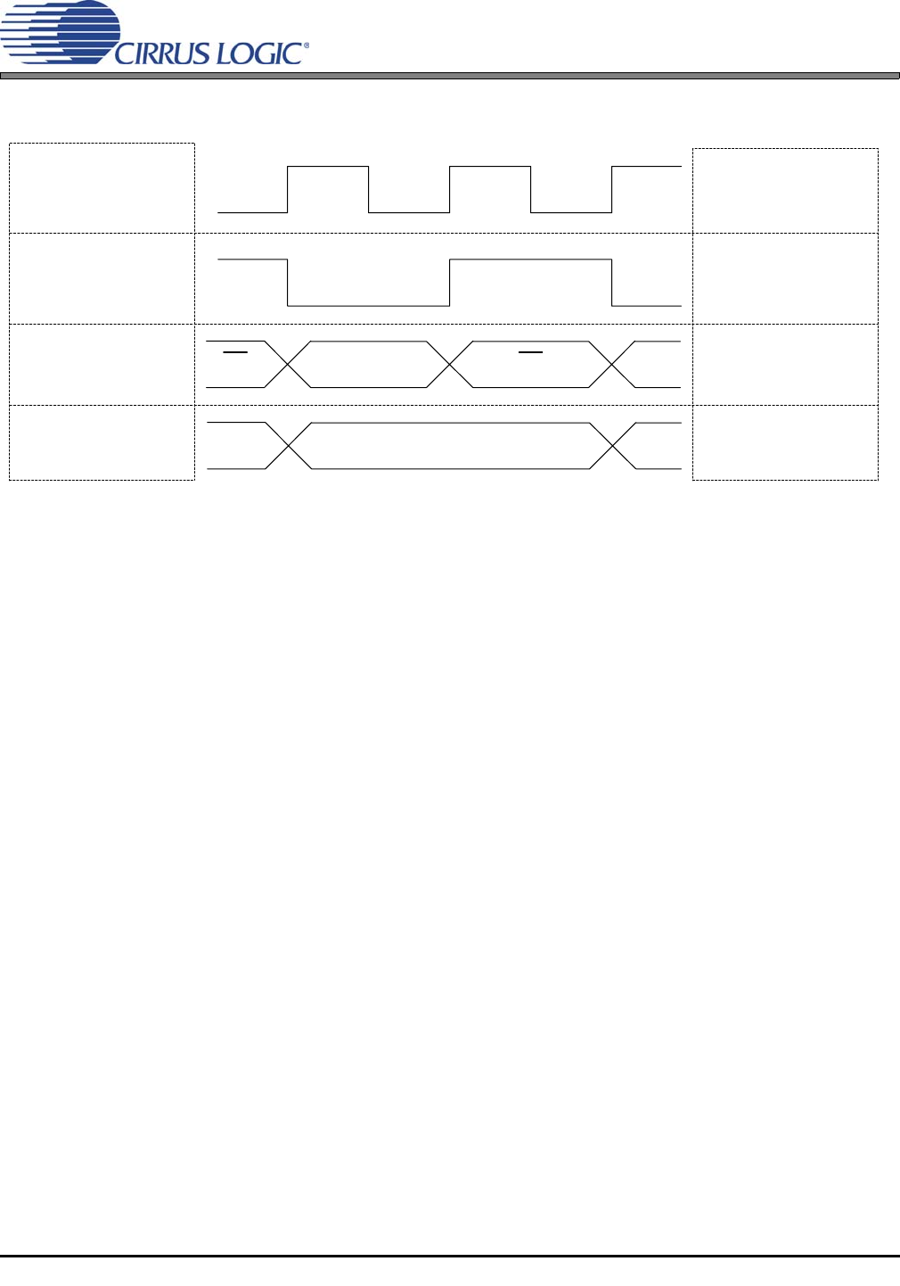
Figure 18. DSD Phase Modulation Mode Diagram
4.9 Grounding and Power Supply Arrangements
As with any high resolution converter, the CS4364 requires careful attention to power supply and grounding
arrangements if its potential performance is to be realized. The Typical Connection Diagram shows the rec-
ommended power arrangements, with VA, VD, VLC, and VLS connected to clean supplies. If the ground
planes are split between digital ground and analog ground, the GND pins of the CS4364 should be connect-
ed to the analog ground plane.
All signals, especially clocks, should be kept away from the FILT+ and VQ pins in order to avoid unwanted
coupling into the DAC.
4.9.1 Capacitor Placement
Decoupling capacitors should be placed as close to the DAC as possible, with the low value ceramic ca-
pacitor being the closest. To further minimize impedance, these capacitors should be located on the same
layer as the DAC. If desired, all supply pins with similar voltage ratings may be connected to the same
supply, but a decoupling capacitor should still be placed on each supply pin.
Note: All decoupling capacitors should be referenced to analog ground.
The CDB4364 evaluation board demonstrates the optimum layout and power supply arrangements.
4.10 Analog Output and Filtering
The CS4364 does not include phase or amplitude compensation for an external filter. Therefore, the DAC
system phase and amplitude response will be dependent on the external analog circuitry.
Figure 19 shows how the full-scale analog output level specification is derived.
Figure 20 shows how the recommended output filtering with location for optional mute circuit.
BCKA
(128Fs)
BCKD
(64Fs)
DSD_SCLK
DSDAx,
DSDBx
D1
D1
D1D0 D2
D2D0
DSD_SCLK
DSDAx,
DSDBx
BCKA
(64Fs)
DSD_SCLK
DSD Phase
Modulation Mode
DSD Normal Mode
Not Used
Not Used
Not Used