
User Manual


Table Of Contents
- 1. Pin Description
- 2. Characteristics and Specifications
- Recommended Operating Conditions
- Absolute Maximum Ratings
- DAC Analog Characteristics
- Power and Thermal Characteristics
- Combined Interpolation & On-Chip Analog Filter Response
- Combined Interpolation & On-Chip Analog Filter Response
- DSD Combined Digital & On-Chip Analog Filter Response
- Digital Characteristics
- Switching Characteristics - PCM
- Switching Characteristics - DSD
- Switching Characteristics - Control Port - I·C Format
- Switching Characteristics - Control Port - SPI Format
- 3. Typical Connection Diagram
- 4. Applications
- 4.1 Master Clock
- 4.2 Mode Select
- 4.3 Digital Interface Formats
- Figure 8. Format 0 - Left-Justified up to 24-bit Data
- Figure 9. Format 1 - I·S up to 24-bit Data
- Figure 10. Format 2 - Right-Justified 16-bit Data
- Figure 11. Format 3 - Right-Justified 24-bit Data
- Figure 12. Format 4 - Right-Justified 20-bit Data
- Figure 13. Format 5 - Right-Justified 18-bit Data
- 4.3.1 OLM #1
- 4.3.2 OLM #2
- 4.4 Oversampling Modes
- 4.5 Interpolation Filter
- 4.6 De-Emphasis
- 4.7 ATAPI Specification
- 4.8 Direct Stream Digital (DSD) Mode
- 4.9 Grounding and Power Supply Arrangements
- 4.10 Analog Output and Filtering
- 4.11 The MUTEC Outputs
- 4.12 Recommended Power-Up Sequence
- 4.13 Recommended Procedure for Switching Operational Modes
- 4.14 Control Port Interface
- 4.15 Memory Address Pointer (MAP)
- 5. Register Quick Reference
- 6. Register Description
- 6.1 Chip Revision (Address 01h)
- 6.2 Mode Control 1 (Address 02h)
- 6.3 PCM Control (Address 03h)
- 6.4 DSD Control (Address 04h)
- 6.5 Filter Control (Address 05h)
- 6.6 Invert Control (Address 06h)
- 6.7 Group Control (Address 07h)
- 6.8 Ramp and Mute (Address 08h)
- 6.9 Mute Control (Address 09h)
- 6.10 Mixing Control (Address 0Ah, 0Dh, 10h, 13h)
- 6.11 Volume Control (Address 0Bh, 0Ch, 0Eh, 0Fh, 11h, 12h)
- 6.12 PCM Clock Mode (Address 16h)
- 7. Filter Response Plots
- Figure 24. Single-Speed (fast) Stopband Rejection
- Figure 25. Single-Speed (fast) Transition Band
- Figure 26. Single-Speed (fast) Transition Band (detail)
- Figure 27. Single-Speed (fast) Passband Ripple
- Figure 28. Single-Speed (slow) Stopband Rejection
- Figure 29. Single-Speed (slow) Transition Band
- Figure 30. Single-Speed (slow) Transition Band (detail)
- Figure 31. Single-Speed (slow) Passband Ripple
- Figure 32. Double-Speed (fast) Stopband Rejection
- Figure 33. Double-Speed (fast) Transition Band
- Figure 34. Double-Speed (fast) Transition Band (detail)
- Figure 35. Double-Speed (fast) Passband Ripple
- Figure 36. Double-Speed (slow) Stopband Rejection
- Figure 37. Double-Speed (slow) Transition Band
- Figure 38. Double-Speed (slow) Transition Band (detail)
- Figure 39. Double-Speed (slow) Passband Ripple
- Figure 40. Quad-Speed (fast) Stopband Rejection
- Figure 41. Quad-Speed (fast) Transition Band
- Figure 42. Quad-Speed (fast) Transition Band (detail)
- Figure 43. Quad-Speed (fast) Passband Ripple
- Figure 44. Quad-Speed (slow) Stopband Rejection
- Figure 45. Quad-Speed (slow) Transition Band
- Figure 46. Quad-Speed (slow) Transition Band (detail)
- Figure 47. Quad-Speed (slow) Passband Ripple
- 8. References
- 9. Parameter Definitions
- 10. Package Dimensions
- 11. Ordering Information
- 12. Revision History
DS619F1 25
CS4364
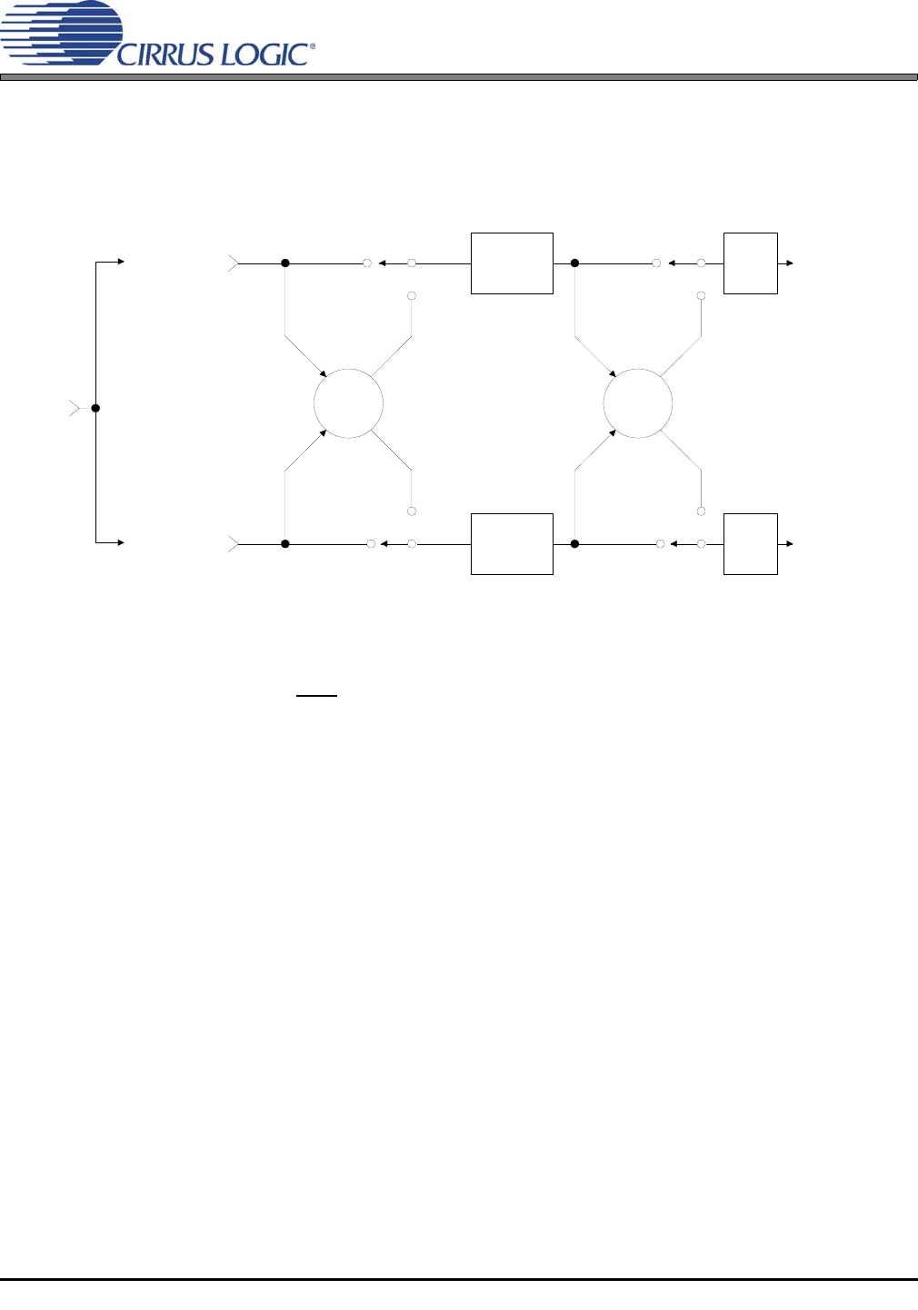
4.7 ATAPI Specification
The CS4364 implements the channel mixing functions of the ATAPI CD-ROM specification. The
ATAPI functions are applied per A-B pair. Refer to Table 9 on page 41 and Figure 17 for additional informa-
tion.
4.8 Direct Stream Digital (DSD) Mode
In Software Mode the DSD/PCM bits (Reg. 02h) are used to configure the device for DSD mode. The
DSD_DIF bits (Reg 04h) then control the expected DSD rate and MCLK ratio.
The DIR_DSD bit (Reg 04h) selects between two proprietary methods for DSD to analog conversion. The
first method uses a decimation free DSD processing technique which allows for features such as matched
PCM level output, DSD volume control, and 50kHz on chip filter. The second method sends the DSD data
directly to the on-chip switched-capacitor filter for conversion (without the above mentioned features).
The DSD_PM_EN bit (Reg. 04h) selects Phase Modulation (data plus data inverted) as the style of data
input. In this mode the DSD_PM_Mode bit selects whether a 128Fs or 64x clock is used for phase modu-
lated 64x data (see Figure 18). Use of Phase Modulation Mode may not directly effect the performance of
the CS4364, but may lower the sensitivity to board level routing of the DSD data signals.
The CS4364 can detect errors in the DSD data which does not comply with the SACD specification. The
STATIC_DSD and INVALID_DSD bits (Reg. 04h) allow the CS4364 to alter the incoming invalid DSD data.
Depending on the error, the data may either be attenuated or replaced with a muted DSD signal (the
MUTEC pins would be set according to the DAMUTE bit (Reg. 08h)).
More information for any of these register bits can be found in the “Parameter Definitions” on page 47.
The DSD input structure and analog outputs are designed to handle a nominal 0 dB-SACD (50% modulation
index) at full rated performance. Signals of +3 dB-SACD may be applied for brief periods of time however,
performance at these levels is not guaranteed. If sustained +3 dB-SACD levels are required, the digital vol-
ume control should be set to -3.0 dB. This same volume control register affects PCM output levels. There
is no need to change the volume control setting between PCM and DSD in order to have the 0 dB output
levels match (both 0 dBFS and 0 dB-SACD will output at -3 dB in this case).
ΣΣ
A Channel
Volume
Control
AoutAx
AoutBx
Left Chan
nel
Audio Data
Right Channel
Audio Data
BChannel
Volume
Control
MUTE
MUTE
SDINx
Figure 17. ATAPI Block Diagram (x = channel pair 1, 2, or 3)