
User Manual


Table Of Contents
- 1. Pin Description
- 2. Characteristics and Specifications
- Recommended Operating Conditions
- Absolute Maximum Ratings
- DAC Analog Characteristics
- Power and Thermal Characteristics
- Combined Interpolation & On-Chip Analog Filter Response
- Combined Interpolation & On-Chip Analog Filter Response
- DSD Combined Digital & On-Chip Analog Filter Response
- Digital Characteristics
- Switching Characteristics - PCM
- Switching Characteristics - DSD
- Switching Characteristics - Control Port - I·C Format
- Switching Characteristics - Control Port - SPI Format
- 3. Typical Connection Diagram
- 4. Applications
- 4.1 Master Clock
- 4.2 Mode Select
- 4.3 Digital Interface Formats
- Figure 8. Format 0 - Left-Justified up to 24-bit Data
- Figure 9. Format 1 - I·S up to 24-bit Data
- Figure 10. Format 2 - Right-Justified 16-bit Data
- Figure 11. Format 3 - Right-Justified 24-bit Data
- Figure 12. Format 4 - Right-Justified 20-bit Data
- Figure 13. Format 5 - Right-Justified 18-bit Data
- 4.3.1 OLM #1
- 4.3.2 OLM #2
- 4.4 Oversampling Modes
- 4.5 Interpolation Filter
- 4.6 De-Emphasis
- 4.7 ATAPI Specification
- 4.8 Direct Stream Digital (DSD) Mode
- 4.9 Grounding and Power Supply Arrangements
- 4.10 Analog Output and Filtering
- 4.11 The MUTEC Outputs
- 4.12 Recommended Power-Up Sequence
- 4.13 Recommended Procedure for Switching Operational Modes
- 4.14 Control Port Interface
- 4.15 Memory Address Pointer (MAP)
- 5. Register Quick Reference
- 6. Register Description
- 6.1 Chip Revision (Address 01h)
- 6.2 Mode Control 1 (Address 02h)
- 6.3 PCM Control (Address 03h)
- 6.4 DSD Control (Address 04h)
- 6.5 Filter Control (Address 05h)
- 6.6 Invert Control (Address 06h)
- 6.7 Group Control (Address 07h)
- 6.8 Ramp and Mute (Address 08h)
- 6.9 Mute Control (Address 09h)
- 6.10 Mixing Control (Address 0Ah, 0Dh, 10h, 13h)
- 6.11 Volume Control (Address 0Bh, 0Ch, 0Eh, 0Fh, 11h, 12h)
- 6.12 PCM Clock Mode (Address 16h)
- 7. Filter Response Plots
- Figure 24. Single-Speed (fast) Stopband Rejection
- Figure 25. Single-Speed (fast) Transition Band
- Figure 26. Single-Speed (fast) Transition Band (detail)
- Figure 27. Single-Speed (fast) Passband Ripple
- Figure 28. Single-Speed (slow) Stopband Rejection
- Figure 29. Single-Speed (slow) Transition Band
- Figure 30. Single-Speed (slow) Transition Band (detail)
- Figure 31. Single-Speed (slow) Passband Ripple
- Figure 32. Double-Speed (fast) Stopband Rejection
- Figure 33. Double-Speed (fast) Transition Band
- Figure 34. Double-Speed (fast) Transition Band (detail)
- Figure 35. Double-Speed (fast) Passband Ripple
- Figure 36. Double-Speed (slow) Stopband Rejection
- Figure 37. Double-Speed (slow) Transition Band
- Figure 38. Double-Speed (slow) Transition Band (detail)
- Figure 39. Double-Speed (slow) Passband Ripple
- Figure 40. Quad-Speed (fast) Stopband Rejection
- Figure 41. Quad-Speed (fast) Transition Band
- Figure 42. Quad-Speed (fast) Transition Band (detail)
- Figure 43. Quad-Speed (fast) Passband Ripple
- Figure 44. Quad-Speed (slow) Stopband Rejection
- Figure 45. Quad-Speed (slow) Transition Band
- Figure 46. Quad-Speed (slow) Transition Band (detail)
- Figure 47. Quad-Speed (slow) Passband Ripple
- 8. References
- 9. Parameter Definitions
- 10. Package Dimensions
- 11. Ordering Information
- 12. Revision History
20 DS619F1
CS4364
4. APPLICATIONS
The CS4364 serially accepts twos complement formatted PCM data at standard audio sample rates including 48,
44.1 and 32 kHz in SSM, 96, 88.2 and 64 kHz in DSM, and 192, 176.4 and 128 kHz in QSM. Audio data is input via
the serial data input pins (SDINx). The Left/Right Clock (LRCK) determines which channel is currently being input
on SDINx, and the Serial Clock (SCLK) clocks audio data into the input data buffer. For more information on serial
audio interfaces see AN282 “The 2-Channel Serial Audio Interface: A Tutorial”.
The CS4364 can be configured in Hardware Mode by the M0, M1, M2, M3 and M4 pins and in Software Mode
through I²C or SPI.
4.1 Master Clock
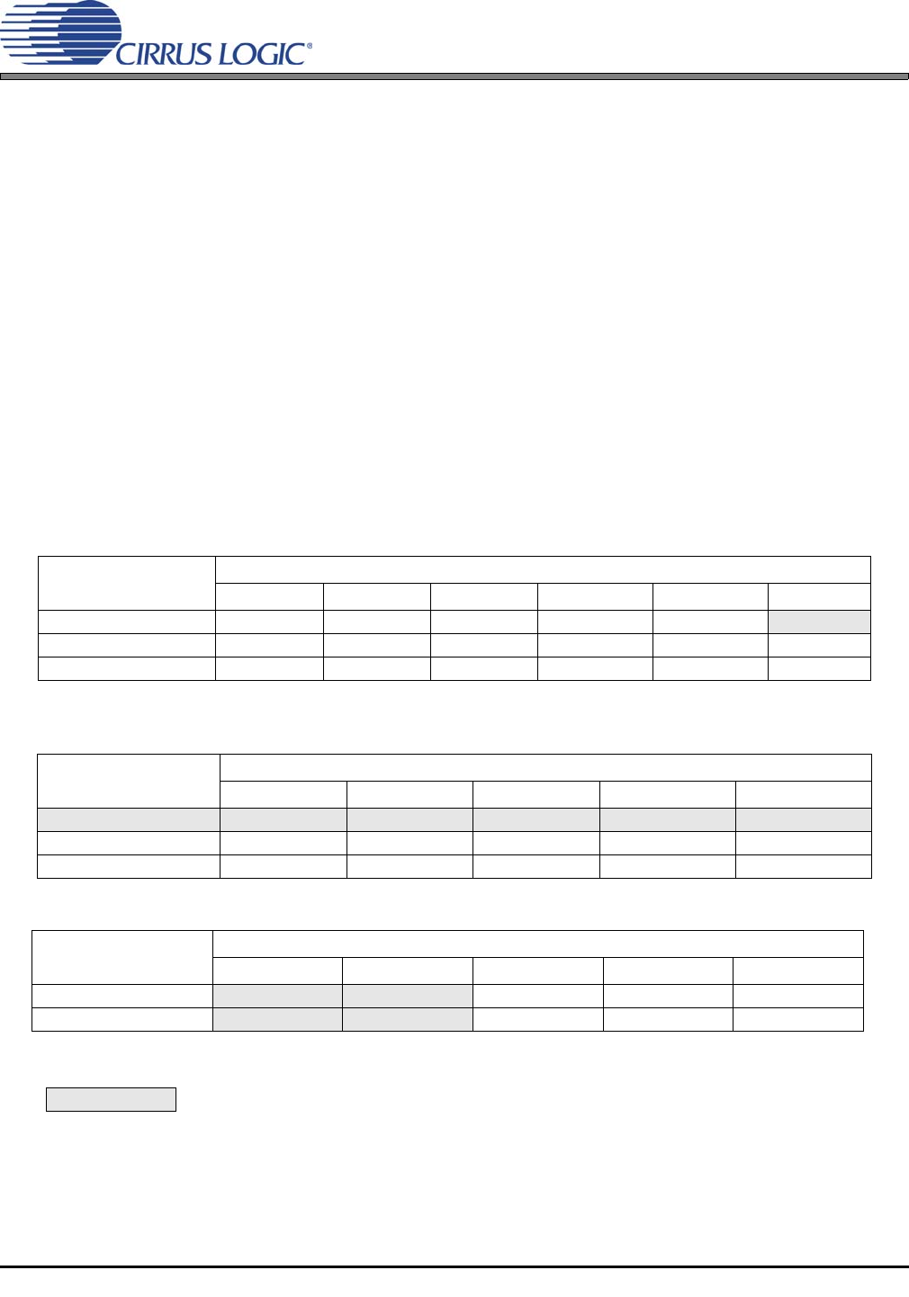
MCLK/LRCK must be an integer ratio as shown in Tables 1 - 3. The LRCK frequency is equal to Fs, the
frequency at which words for each channel are input to the device. The MCLK-to-LRCK frequency ratio and
speed mode is detected automatically during the initialization sequence by counting the number of MCLK
transitions during a single LRCK period and by detecting the absolute speed of MCLK. Internal dividers are
then set to generate the proper internal clocks. Tables 1 - 3 illustrate several standard audio sample rates
and the required MCLK and LRCK frequencies. Please note there is no required phase relationship, but
MCLK, LRCK and SCLK must be synchronous.
Sample Rate
(kHz)
MCLK (MHz)
256x 384x 512x 768x 1024x 1152x
32 8.1920 12.2880 16.3840 24.5760 32.7680 36.8640
44.1 11.2896 16.9344 22.5792 33.8688 45.1584
48 12.2880 18.4320 24.5760 36.8640 49.1520
Table 1. Single-Speed Mode Standard Frequencies
Sample Rate
(kHz)
MCLK (MHz)
128x 192x 256x 384x 512x
64 8.1920 12.2880 16.3840 24.5760 32.7680
88.2 11.2896 16.9344 22.5792 33.8688 45.1584
96 12.2880 18.4320 24.5760 36.8640 49.1520
Table 2. Double-Speed Mode Standard Frequencies
Sample Rate
(kHz)
MCLK (MHz)
64x 96x 128x 192x 256x
176.4 11.2896 16.9344 22.5792 33.8688 45.1584
192
12.2880 18.4320 24.5760 36.8640 49.1520
Table 3. Quad-Speed Mode Standard Frequencies
= Denotes clock ratio and sample rate combinations which are NOT supported under auto
speed-mode detection. Please see “Switching Characteristics - PCM” on page 14.