
User Manual


Table Of Contents
- 1. Pin Description
- 2. Characteristics and Specifications
- Recommended Operating Conditions
- Absolute Maximum Ratings
- DAC Analog Characteristics
- Power and Thermal Characteristics
- Combined Interpolation & On-Chip Analog Filter Response
- Combined Interpolation & On-Chip Analog Filter Response
- DSD Combined Digital & On-Chip Analog Filter Response
- Digital Characteristics
- Switching Characteristics - PCM
- Switching Characteristics - DSD
- Switching Characteristics - Control Port - I·C Format
- Switching Characteristics - Control Port - SPI Format
- 3. Typical Connection Diagram
- 4. Applications
- 4.1 Master Clock
- 4.2 Mode Select
- 4.3 Digital Interface Formats
- Figure 8. Format 0 - Left-Justified up to 24-bit Data
- Figure 9. Format 1 - I·S up to 24-bit Data
- Figure 10. Format 2 - Right-Justified 16-bit Data
- Figure 11. Format 3 - Right-Justified 24-bit Data
- Figure 12. Format 4 - Right-Justified 20-bit Data
- Figure 13. Format 5 - Right-Justified 18-bit Data
- 4.3.1 OLM #1
- 4.3.2 OLM #2
- 4.4 Oversampling Modes
- 4.5 Interpolation Filter
- 4.6 De-Emphasis
- 4.7 ATAPI Specification
- 4.8 Direct Stream Digital (DSD) Mode
- 4.9 Grounding and Power Supply Arrangements
- 4.10 Analog Output and Filtering
- 4.11 The MUTEC Outputs
- 4.12 Recommended Power-Up Sequence
- 4.13 Recommended Procedure for Switching Operational Modes
- 4.14 Control Port Interface
- 4.15 Memory Address Pointer (MAP)
- 5. Register Quick Reference
- 6. Register Description
- 6.1 Chip Revision (Address 01h)
- 6.2 Mode Control 1 (Address 02h)
- 6.3 PCM Control (Address 03h)
- 6.4 DSD Control (Address 04h)
- 6.5 Filter Control (Address 05h)
- 6.6 Invert Control (Address 06h)
- 6.7 Group Control (Address 07h)
- 6.8 Ramp and Mute (Address 08h)
- 6.9 Mute Control (Address 09h)
- 6.10 Mixing Control (Address 0Ah, 0Dh, 10h, 13h)
- 6.11 Volume Control (Address 0Bh, 0Ch, 0Eh, 0Fh, 11h, 12h)
- 6.12 PCM Clock Mode (Address 16h)
- 7. Filter Response Plots
- Figure 24. Single-Speed (fast) Stopband Rejection
- Figure 25. Single-Speed (fast) Transition Band
- Figure 26. Single-Speed (fast) Transition Band (detail)
- Figure 27. Single-Speed (fast) Passband Ripple
- Figure 28. Single-Speed (slow) Stopband Rejection
- Figure 29. Single-Speed (slow) Transition Band
- Figure 30. Single-Speed (slow) Transition Band (detail)
- Figure 31. Single-Speed (slow) Passband Ripple
- Figure 32. Double-Speed (fast) Stopband Rejection
- Figure 33. Double-Speed (fast) Transition Band
- Figure 34. Double-Speed (fast) Transition Band (detail)
- Figure 35. Double-Speed (fast) Passband Ripple
- Figure 36. Double-Speed (slow) Stopband Rejection
- Figure 37. Double-Speed (slow) Transition Band
- Figure 38. Double-Speed (slow) Transition Band (detail)
- Figure 39. Double-Speed (slow) Passband Ripple
- Figure 40. Quad-Speed (fast) Stopband Rejection
- Figure 41. Quad-Speed (fast) Transition Band
- Figure 42. Quad-Speed (fast) Transition Band (detail)
- Figure 43. Quad-Speed (fast) Passband Ripple
- Figure 44. Quad-Speed (slow) Stopband Rejection
- Figure 45. Quad-Speed (slow) Transition Band
- Figure 46. Quad-Speed (slow) Transition Band (detail)
- Figure 47. Quad-Speed (slow) Passband Ripple
- 8. References
- 9. Parameter Definitions
- 10. Package Dimensions
- 11. Ordering Information
- 12. Revision History
18 DS619F1
CS4364
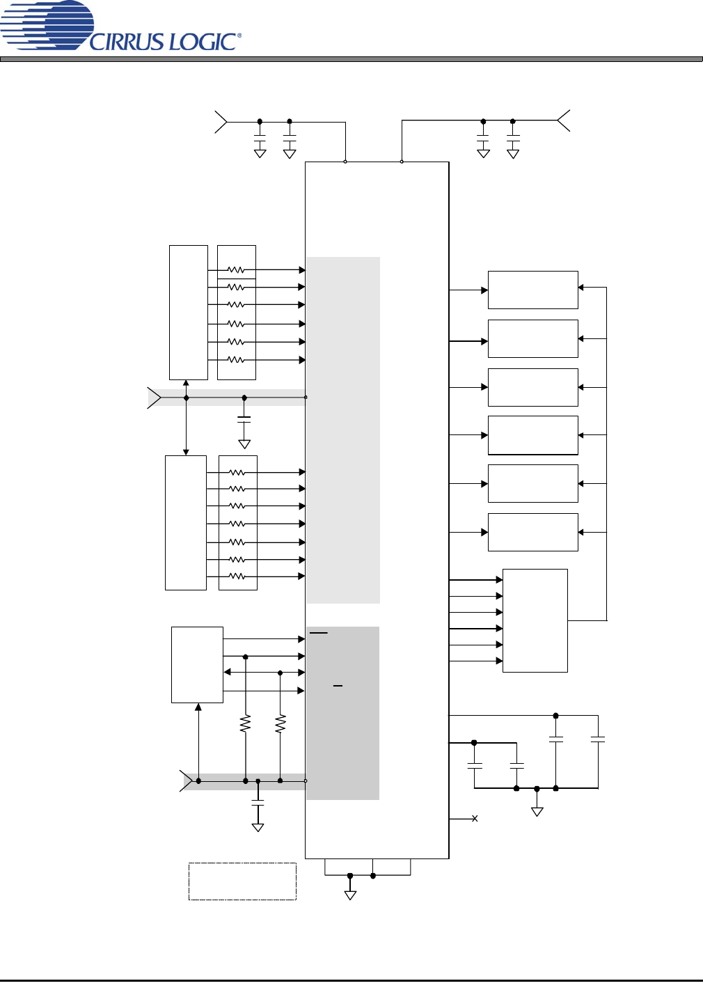
3. TYPICAL CONNECTION DIAGRAM
VLS
MCL K
VD
AOUT1
8
32
0.1 µF
+
1 µF
+2.5 V
SDIN1
9
1 µF
0.1 µ
F
+
+
20
21
FILT+
CMOUT
7
6
LRCK
SCLK
SDIN3
SDIN2
39
0.1 µ
F
47 µF
VA
0.1 µF
+
1 µF
0.1 µF
+1.8 V to +5 V
+5 V
4
43
13
Analog Conditioning
and Muting
AOUT2
38
Analog Conditioning
and Muting
AOUT3
35
Analog Conditioning
and Muting
AOUT4
34
Analog Conditioning
and Muting
AOUT5
29
Analog Conditioning
and Muting
AOUT6
28
Analog Conditioning
and Muting
MUT EC1
41
26
Mu t e
Dr iv e
MUT EC2
11
Mi c r o -
Controller
VLC
0.1 µF
+1.8 V to +5 V
18
2
48
DSD4
3
42
DSD_SCLK
DSD1
DSD6
DSD5
DSD2
DSD3
46
47
1
16
15
SCL/ CCLK
SDA/CDIN
ADO/CS
RST
19
17
2 K Ω
2 K
Ω
Note*: Necessary for
I
2
C
control port
operation
Not e*
MUT EC3
25
24
MUT EC4
MUTEC5
23
22
MUT EC6
CS4364
31
GND
GND
5
TST*
DSD
Audio
Source
220 Ω
470 Ω
470 Ω
Dig it al
Audio
Source
PCM
*Pins: 10, 12,
14, 44, 45
Pins: 27, 30, 33,
36, 37, 40
TST_OUT
Figure 6. Typical Connection Diagram, Software Mode