CS4364 103 dB, 192 kHz 6-Channel D/A Converter Features Description Advanced Multi-bit Delta Sigma Architecture The CS4364 is a complete 6-channel digital-to-analog system. This D/A system includes digital de-emphasis, half-dB step size volume control, ATAPI channel mixing, selectable fast and slow digital interpolation filters followed by an oversampled, multi-bit delta sigma modulator which includes mismatch shaping technology that eliminates distortion due to capacitor mismatch.
CS4364 TABLE OF CONTENTS 1. PIN DESCRIPTION................................................................................................................................. 6 2. CHARACTERISTICS AND SPECIFICATIONS...................................................................................... 8 RECOMMENDED OPERATING CONDITIONS .......................................................................................... 8 ABSOLUTE MAXIMUM RATINGS.............................................................
CS4364 6.3 PCM Control (Address 03h) .......................................................................................................... 34 6.3.1 Digital Interface Format (DIF)............................................................................................... 34 6.3.2 Functional Mode (FM) .......................................................................................................... 35 6.4 DSD Control (Address 04h) ...............................................................
CS4364 LIST OF FIGURES Figure 1. Serial Audio Interface Timing...................................................................................................... 14 Figure 2. Direct Stream Digital - Serial Audio Input Timing........................................................................ 15 Figure 3. Direct Stream Digital - Serial Audio Input Timing for Phase Modulation Mode........................... 15 Figure 4. Control Port Timing - I²C Format...................................................
CS4364 LIST OF TABLES Table 1. Single-Speed Mode Standard Frequencies ................................................................................ Table 2. Double-Speed Mode Standard Frequencies............................................................................... Table 3. Quad-Speed Mode Standard Frequencies ................................................................................. Table 4. PCM Digital Interface Format, Hardware Mode Options..............................................
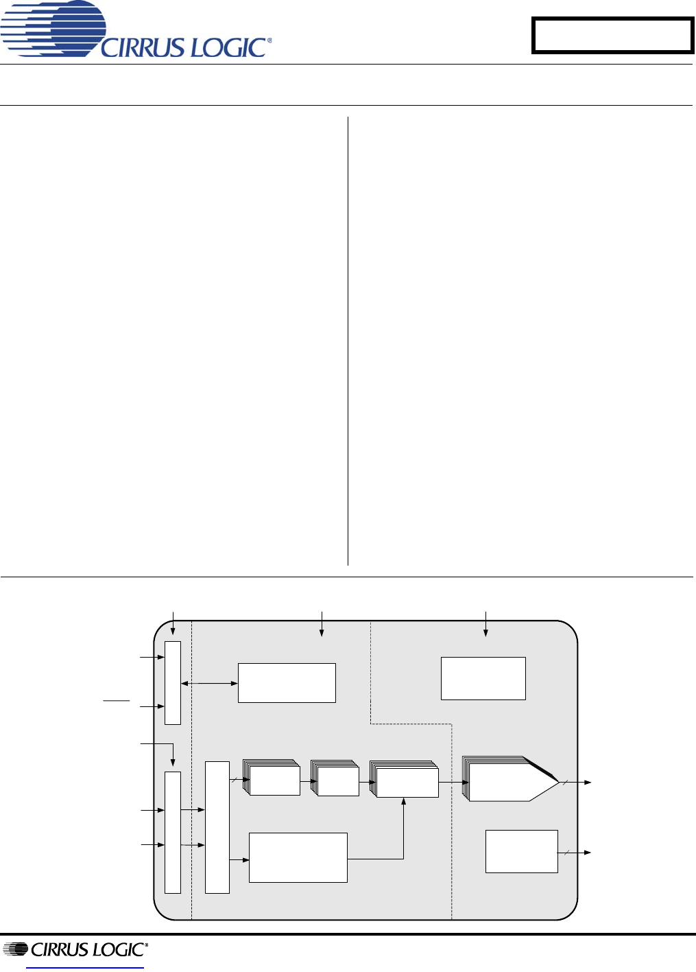
CS4364 TST_OUT DSD_SCLK MUTE1 TST_OUT AOUT1 AOUT2 DSD4 DSD5 DSD6 TST TST VLS 1.
CS4364 Pin Name # Pin Description FILT+ 20 Positive Voltage Reference (Output) - Positive reference voltage for the internal sampling circuits. Requires the capacitive decoupling to analog ground as shown in the Typical Connection Diagram. AOUT1 AOUT2 AOUT3 AOUT4 AOUT5 AOUT6 39 38 35 34 29 28 Analog Output (Output) - The full scale analog output level is specified in the Analog Characteristics specification table.
CS4364 2. CHARACTERISTICS AND SPECIFICATIONS RECOMMENDED OPERATING CONDITIONS (GND = 0 V; all voltages with respect to ground.) Parameters Symbol Min Typ Max Units Analog power Digital internal power Serial data port interface power Control port interface power Ambient Operating Temperature (Power Applied) -CQZ VA VD VLS VLC TA 4.75 2.37 1.71 1.71 -40 5.0 2.5 5.0 5.0 - 5.25 2.63 5.25 5.25 +85 V V V V °C DC Power Supply ABSOLUTE MAXIMUM RATINGS (GND = 0 V; all voltages with respect to ground.
CS4364 DAC ANALOG CHARACTERISTICS Test Conditions (unless otherwise indicated): VA = VLS = VLC = 5 V; VD = 2.5 V; TA = 25 °C; Full-Scale 997 Hz input sine wave (Note 1); Tested under max ac-load resistance; Valid with FILT+ and VQ capacitors as shown in “Typical Connection Diagram” on page 18; Measurement Bandwidth 10 Hz to 20 kHz.
CS4364 POWER AND THERMAL CHARACTERISTICS Parameters Symbol Min Typ Max Units normal operation, VA= 5 V VD= 2.5 V (Note 5) Interface current, VLC=5 V VLS=5 V (Note 6) power-down state (all supplies) Power Dissipation (Note 4) VA = 5 V, VD = 2.
CS4364 COMBINED INTERPOLATION & ON-CHIP ANALOG FILTER RESPONSE The filter characteristics have been normalized to the sample rate (Fs) and can be referenced to the desired sample rate by multiplying the given characteristic by Fs. (See (Note 12)) Fast Roll-Off Parameter Min Typ Combined Digital and On-chip Analog Filter Response - Single-Speed Mode - 48 kHz Passband (Note 9) Frequency Response StopBand StopBand Attenuation Group Delay De-emphasis Error (Note 11) (Relative to 1 kHz) to -0.
CS4364 COMBINED INTERPOLATION & ON-CHIP ANALOG FILTER RESPONSE (CONTINED) Slow Roll-Off (Note 8) Min Typ Max Parameter Single-Speed Mode - 48 kHz Passband (Note 9) to -0.01 dB corner to -3 dB corner 10 Hz to 20 kHz Frequency Response StopBand StopBand Attenuation Group Delay De-emphasis Error (Note 11) (Relative to 1 kHz) (Note 10) Fs = 32 kHz Fs = 44.1 kHz Fs = 48 kHz Unit 0 0 -0.01 .583 64 - 7.8/Fs - 0.417 0.499 +0.01 ±0.36 ±0.21 ±0.14 Fs Fs dB Fs dB s dB dB dB 0 0 -0.01 .792 70 - 5.4/Fs .
CS4364 DIGITAL CHARACTERISTICS Parameters Input Leakage Current Input Capacitance High-Level Input Voltage (Note 13) Serial I/O Control I/O Low-Level Input Voltage Serial I/O Control I/O Low-Level Output Voltage (IOL = -1.2 mA) Control I/O = 3.3 V, 5 V Control I/O = 1.8 V, 2.
CS4364 SWITCHING CHARACTERISTICS - PCM (Inputs: Logic 0 = GND, Logic 1 = VLS, CL = 30 pF) Parameters Symbol RST pin Low Pulse Width (Note 14) MCLK Frequency MCLK Duty Cycle (Note 15) Min Max Units 1 - ms 1.024 55.
CS4364 SWITCHING CHARACTERISTICS - DSD (Logic 0 = AGND = DGND; Logic 1 = VLS; CL = 30 pF) Parameter Symbol MCLK Duty Cycle DSD_SCLK Pulse Width Low DSD_SCLK Pulse Width High DSD_SCLK Frequency tsclkl tsclkh (64x Oversampled) (128x Oversampled) DSD_A / _B valid to DSD_SCLK rising setup time DSD_SCLK rising to DSD_A or DSD_B hold time DSD clock to data transition (Phase Modulation Mode) tsdlrs tsdh tdpm Min Typ Max Unit 40 160 160 1.024 2.048 20 20 -20 - 60 3.2 6.
CS4364 SWITCHING CHARACTERISTICS - CONTROL PORT - I²C FORMAT (Inputs: Logic 0 = GND, Logic 1 = VLC, CL = 30 pF) Parameter Symbol Min Max Unit SCL Clock Frequency fscl - 100 kHz RST Rising Edge to Start tirs 500 - ns Bus Free Time Between Transmissions tbuf 4.7 - µs Start Condition Hold Time (prior to first clock pulse) thdst 4.0 - µs Clock Low time tlow 4.7 - µs Clock High Time thigh 4.0 - µs Setup Time for Repeated Start Condition tsust 4.
CS4364 SWITCHING CHARACTERISTICS - CONTROL PORT - SPI FORMAT (Inputs: Logic 0 = GND, Logic 1 = VLC, CL = 30 pF) Parameter Symbol Min Max Unit CCLK Clock Frequency fsclk - 6 MHz RST Rising Edge to CS Falling tsrs 500 - ns tspi 500 - ns CS High Time Between Transmissions tcsh 1.
CS4364 3. TYPICAL CONNECTION DIAGRAM +2.5 V +5 V 1 µF + + 0.1 µF 0.
CS4364 +2.5 V +5 V 1 µF + 0.1 µF 0.1 µF 6 7 PCM Digital Audio Source 9 8 11 13 MCLK AOUT1 LRCK SCLK MUTEC1 43 SDIN3 AOUT2 2 1 DSD Audio Source 48 47 46 42 MUTEC2 Stand-Alone Mode Configuration MUTEC3 AOUT4 MUTEC4 DSDA3 DSD_SCLK Analog Conditioning and Muting 34 24 Analog Conditioning and Muting 29 23 Analog Conditioning and Muting M4 M3 M2 AOUT6 M1 MUTEC6 28 22 Analog Conditioning and Muting M0 RST FILT+ CMOUT +1.
CS4364 4. APPLICATIONS The CS4364 serially accepts twos complement formatted PCM data at standard audio sample rates including 48, 44.1 and 32 kHz in SSM, 96, 88.2 and 64 kHz in DSM, and 192, 176.4 and 128 kHz in QSM. Audio data is input via the serial data input pins (SDINx). The Left/Right Clock (LRCK) determines which channel is currently being input on SDINx, and the Serial Clock (SCLK) clocks audio data into the input data buffer.
CS4364 4.2 Mode Select In Hardware Mode, operation is determined by the Mode Select pins. The states of these pins are continually scanned for any changes; however, the mode should only be changed while the device is in reset (RST pin low) to ensure proper switching from one mode to another. These pins require connection to supply or ground as outlined in Figure 7. For M0, M1, and M2, supply is VLC. For M3 and M4, supply is VLS. Tables 4 - 6 show the decode of these pins.
CS4364 4.3 Digital Interface Formats The serial port operates as a slave and supports the I²S, Left-Justified, Right-Justified, and One-Line Mode (OLM) digital interface formats with varying bit depths from 16 to 32 as shown in Figures 8-15. Data is clocked into the DAC on the rising edge. OLM configurations are only supported in Software Mode. Left Channel LRCK Right Channel SCLK SDINx MSB -1 -2 -3 -4 -5 +5 +4 +3 +2 +1 LSB MSB -1 -2 -3 -4 +5 +4 +3 +2 +1 LSB Figure 8.
CS4364 LRCK Right Channel Left Channel SCLK SDINx 1 0 17 16 15 14 13 12 11 10 9 8 7 6 5 4 3 2 1 0 17 16 15 14 13 12 11 10 9 8 7 6 5 4 3 2 1 0 32 clocks Figure 13. Format 5 - Right-Justified 18-bit Data 4.3.1 OLM #1 OLM #1 serial audio interface format operates in Single-, Double-, or Quad-Speed Mode and will slave to SCLK at 128 Fs. Six channels of MSB first 20-bit PCM data are input on SDIN1.
CS4364 4.5 Interpolation Filter To accommodate the increasingly complex requirements of digital audio systems, the CS4364 incorporates selectable interpolation filters for each mode of operation. A “fast” and a “slow” roll-off filter is available in each of Single-, Double-, or Quad-Speed Modes. These filters have been designed to accommodate a variety of musical tastes and styles. The FILT_SEL bit is used to select which filter is used (see the “Parameter Definitions” on page 47 for more details).
CS4364 4.7 ATAPI Specification The CS4364 implements the channel mixing functions of the ATAPI CD-ROM specification. The ATAPI functions are applied per A-B pair. Refer to Table 9 on page 41 and Figure 17 for additional information. A Channel Volume Control Left Channel Audio Data Σ SDINx Aout Ax MUTE AoutBx Σ B Channel Volume Control Right Channel Audio Data MUTE Figure 17. ATAPI Block Diagram (x = channel pair 1, 2, or 3) 4.
CS4364 DSD Phase Modulation Mode DSD Normal Mode BCKA (64Fs) Not Used DSD_SCLK BCKA (128Fs) DSD_SCLK DSD_SCLK BCKD (64Fs) Not Used DSDAx, DSDBx D0 D1 D1 D0 D1 D2 D2 DSDAx, DSDBx Not Used Figure 18. DSD Phase Modulation Mode Diagram 4.9 Grounding and Power Supply Arrangements As with any high resolution converter, the CS4364 requires careful attention to power supply and grounding arrangements if its potential performance is to be realized.
CS4364 4.175 V 2.5 V AOUT 0.825 V Full-Scale Output Level= AOUT= 3.35 Vpp Figure 19. Full-Scale Output Figure 20. Recommended Output Filter 4.11 The MUTEC Outputs The MUTEC1 pins have an auto-polarity detect feature. The MUTEC output pins are high impedance at the time of reset. The external mute circuitry needs to be self biased into an active state in order to be muted during reset.
CS4364 Figure 21. Recommended Mute Circuitry 4.12 Recommended Power-Up Sequence 4.12.1 Hardware Mode 1. Hold RST low until the power supplies and configuration pins are stable, and the master and left/right clocks are locked to the appropriate frequencies, as discussed in Section 4.1. In this state, the registers are reset to the default settings, FILT+ will remain low, and VQ will be connected to VA/2.
CS4364 converted incorrectly by the Hardware Mode settings). 4. Set the PDN bit to 0. This will initiate the power-up sequence, which lasts approximately 50 µs. 4.13 Recommended Procedure for Switching Operational Modes For systems where the absolute minimum in clicks and pops is required, it is recommended that the MUTE bits are set prior to changing significant DAC functions (such as changing sample rates or clock sources).
CS4364 4.14.2.2 I²C Read To read from the device, follow the procedure below while adhering to the control port Switching Specifications. 1. Initiate a START condition to the I²C bus followed by the address byte. The upper 6 bits must be 001100. The seventh bit must match the setting of the AD0 pin, and the eighth must be 1. The eighth bit of the address byte is the R/W bit. 2. After transmitting an acknowledge (ACK), the device will then transmit the contents of the register pointed to by the MAP.
CS4364 6. If the INCR bit is set to 0 and further SPI writes to other registers are desired, it is necessary to bring CS high, and follow the procedure detailed from step 1. If no further writes to other registers are desired, bring CS high. CS C C LK C H IP ADDRESS C DIN 0011000 MAP D A TA LSB MSB R /W byte 1 byte n M A P = M em ory A d dress P oin te r Figure 23. Control Port Timing, SPI Mode 4.
CS4364 5. REGISTER QUICK REFERENCE Addr 01h Function Chip Revision default 02h Mode Control default 03h PCM Control default 04h DSD Control 05h Filter Control 06h Invert Control 07h Group Control 08h Ramp and Mute 09h Mute Control default default default default default default 0Ah Mixing Control Pair 1 (AOUTx1) default 0Bh Vol. Control A1 default 0Ch Vol. Control B1 default 0Dh Mixing Control Pair 2 (AOUTx1) default 0Eh Vol. Control A2 default 0Fh Vol.
CS4364 6. REGISTER DESCRIPTION Note: All registers are read/write in I²C Mode and write only in SPI, unless otherwise noted. 6.1 Chip Revision (Address 01h) 7 PART4 0 6.1.1 6 PART3 1 5 PART2 1 4 PART1 0 3 PART0 0 2 REV2 - 1 REV1 - 0 REV0 - Part Number ID (PART) [Read Only] 01100 - CS4364 6.1.2 Revision ID (REV) [Read Only] 000 - Revision A0 001 - Revision B0 Function: This read-only register can be used to identify the model and revision number of the device. 6.
CS4364 6.2.3 PCM/DSD Selection (DSD/PCM) Default = 0 0 - PCM 1 - DSD Function: This function selects DSD or PCM Mode. The appropriate data and clocks should be present before changing modes, or else MUTE should be selected. 6.2.4 DAC Pair Disable (DACx_DIS) Default = 0 0 - DAC Pair x Enabled 1 - DAC Pair x Disabled Function: When the bit is set, the respective DAC channel pair (AOUTAx and AOUTBx) will remain in a reset state.
CS4364 DIF3 DIF2 DIF1 DIF0 0 0 0 0 0 0 1 1 X 0 0 0 0 1 1 0 0 X 0 0 1 1 0 0 0 0 X 0 1 0 1 0 1 0 1 X DESCRIPTION Left Justified, up to 24-bit data I2S, up to 24-bit data Right Justified, 16-bit data Right Justified, 24-bit data Right Justified, 20-bit data Right Justified, 18-bit data One-line Mode 1, 24-bit Data One-line Mode 2, 20-bit Data All other combinations are Reserved Format FIGURE 0 1 2 3 4 5 8 9 8 9 10 11 12 13 14 15 Table 7. Digital Interface Formats - PCM Mode 6.3.
CS4364 6.4.2 Direct DSD Conversion (DIR_DSD) Function: When set to 0 (default), DSD input data is sent to the DSD processor for filtering and volume control functions. When set to 1, DSD input data is sent directly to the switched capacitor DACs for a pure DSD conversion.
CS4364 6.5 Filter Control (Address 05h) 7 Reserved 0 6.5.1 6 Reserved 0 5 Reserved 0 4 Reserved 0 3 Reserved 0 2 Reserved 0 1 Reserved 0 0 FILT_SEL 0 Interpolation Filter Select (FILT_SEL) Function: When set to 0 (default), the Interpolation Filter has a fast roll off. When set to 1, the Interpolation Filter has a slow roll off. The specifications for each filter can be found in the Analog characteristics table, and response plots can be found in Figures 22 to 45. 6.
CS4364 Function: The AOUTAx and AOUTBx volume levels are independently controlled by the A and the B Channel Volume Control Bytes when this function is disabled. The volume on both AOUTAx and AOUTBx are determined by the A Channel Attenuation and Volume Control Bytes (per A-B pair), and the B Channel Bytes are ignored when this function is enabled. 6.7.
CS4364 sample rate) if the signal does not encounter a zero crossing. The zero cross function is independently monitored and implemented for each channel. 6.8.2 Soft Volume Ramp-Up After Error (RMP_UP) Function: An un-mute will be performed after executing an LRCK/MCLK ratio change or error, and after changing the Functional Mode. When set to 1 (default), this un-mute is effected, similar to attenuation changes, by the Soft and Zero Cross bits in the Volume and Mixing Control register.
CS4364 6.8.6 MUTE Polarity and DETECT (MUTEP1:0) Default = 00 00 - Auto polarity detect, selected from MUTEC1 pin 01 - Reserved 10 - Active low mute polarity 11 - Active high mute polarity Function: Auto mute polarity detect (00) See Section 4.11 on page 27 for the description. Active low mute polarity (10) When RST is low the outputs are high impedance and will need to be biased active. Once reset has been released and after this bit is set, the MUTEC output pins will be active low polarity.
CS4364 Selects the appropriate digital filter to maintain the standard 15 µs/50 µs digital de-emphasis filter response at 32, 44.1 or 48 kHz sample rates. (Figure 16 on page 24) De-emphasis is only available in Single-Speed Mode. 6.10.2 ATAPI Channel Mixing and Muting (ATAPI) Default = 01001 - AOUTAx=aL, AOUTBx=bR (Stereo) Function: The CS4364 implements the channel mixing functions of the ATAPI CD-ROM specification. The ATAPI functions are applied per A-B pair.
CS4364 6.11 Volume Control (Address 0Bh, 0Ch, 0Eh, 0Fh, 11h, 12h) 7 xx_VOL7 0 6 xx_VOL6 0 5 xx_VOL5 0 4 xx_VOL4 0 3 xx_VOL3 0 2 xx_VOL2 0 1 xx_VOL1 0 0 xx_VOL0 0 These six registers provide individual volume and mute control for each of the six channels.
CS4364 0 0 −20 −20 −40 −40 Amplitude (dB) Amplitude (dB) 7. FILTER RESPONSE PLOTS −60 −60 −80 −80 −100 −100 −120 0.4 0.5 0.6 0.7 0.8 Frequency(normalized to Fs) 0.9 −120 0.4 1 Figure 24. Single-Speed (fast) Stopband Rejection 0.42 0.44 0.46 0.48 0.5 0.52 Frequency(normalized to Fs) 0.54 0.56 0.58 0.6 Figure 25. Single-Speed (fast) Transition Band 0.02 0 −1 0.015 −2 0.01 0.005 −4 Amplitude (dB) Amplitude (dB) −3 −5 −6 0 −0.005 −7 −0.01 −8 −0.015 −9 −10 0.45 0.
CS4364 0.02 0 −1 0.015 −2 0.01 0.005 −4 Amplitude (dB) Amplitude (dB) −3 −5 −6 0 −0.005 −7 −0.01 −8 −0.015 −9 −10 0.45 0.46 0.47 0.48 0.49 0.5 0.51 Frequency(normalized to Fs) 0.52 0.53 0.54 −0.02 0.55 Figure 30. Single-Speed (slow) Transition Band (detail) 0.1 0.15 0.2 0.25 0.3 Frequency(normalized to Fs) 0.35 0.4 0.45 0.5 0 20 20 40 40 Amplitude (dB) Amplitude (dB) 0.05 Figure 31. Single-Speed (slow) Passband Ripple 0 60 60 80 80 100 100 120 0 120 0.
CS4364 0 20 20 40 40 Amplitude (dB) Amplitude (dB) 0 60 60 80 80 100 100 120 120 0.2 0.3 0.4 0.5 0.6 0.7 Frequency(normalized to Fs) 0.8 0.9 1 Figure 36. Double-Speed (slow) Stopband Rejection 0.2 0.3 0.4 0.5 0.6 Frequency(normalized to Fs) 0.7 0.8 Figure 37. Double-Speed (slow) Transition Band 0 0.02 1 0.015 2 0.01 0.005 4 Amplitude (dB) Amplitude (dB) 3 5 6 0 0.005 7 0.01 8 0.015 9 10 0.45 0.46 0.47 0.48 0.49 0.5 0.51 Frequency(normalized to Fs) 0.52 0.
CS4364 0.2 0 1 0.15 2 0.1 3 Amplitude (dB) Amplitude (dB) 0.05 4 5 6 0 0.05 7 0.1 8 0.15 9 10 0.45 0.2 0.46 0.47 0.48 0.49 0.5 0.51 Frequency(normalized to Fs) 0.52 0.53 0.54 0.55 Figure 42. Quad-Speed (fast) Transition Band (detail) 0 0.05 0.1 0.15 Frequency(normalized to Fs) 0.2 0.25 Figure 43. Quad-Speed (fast) Passband Ripple 0 0 20 40 40 Amplitude (dB) Amplitude (dB) 20 60 60 80 80 100 100 120 120 0.1 0.2 0.3 0.4 0.5 0.6 0.
CS4364 8. REFERENCES 1. How to Achieve Optimum Performance from Delta-Sigma A/D & D/A Converters, by Steven Harris. Paper presented at the 93rd Convention of the Audio Engineering Society, October 1992. 2. CDB4364 data sheet, available at http://www.cirrus.com. 3. Design Notes for a 2-Pole Filter with Differential Input, by Steven Green. Cirrus Logic Application Note AN48 4. The I²C-Bus Specification: Version 2.0, Philips Semiconductors, December 1998. http://www.semiconductors.philips.com 5.
CS4364 10.PACKAGE DIMENSIONS 48L LQFP PACKAGE DRAWING E E1 D D1 1 e B ∝ A A1 L DIM MIN INCHES NOM MAX MIN MILLIMETERS NOM MAX A A1 B D D1 E E1 e* L --0.002 0.007 0.343 0.272 0.343 0.272 0.016 0.018 0.000° 0.055 0.004 0.009 0.354 0.28 0.354 0.28 0.020 0.24 4° 0.063 0.006 0.011 0.366 0.280 0.366 0.280 0.024 0.030 7.000° --0.05 0.17 8.70 6.90 8.70 6.90 0.40 0.45 0.00° 1.40 0.10 0.22 9.0 BSC 7.0 BSC 9.0 BSC 7.0 BSC 0.50 BSC 0.60 4° 1.60 0.15 0.27 9.30 7.10 9.30 7.10 0.60 0.75 7.
CS4364 11.
CS4364 12.