
User Manual
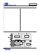


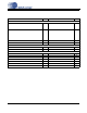

DS617F2 7
CS4362A
VQ 21
Quiescent Voltage (Output) - Filter conne ction for internal quiescent voltage. VQ must be
capacitively coupled to analog ground, as shown in the Typical Connection Diagram. The nom-
inal voltage level is specified in the Analog Characteristics and Speci fica ti ons section. VQ pre-
sents an appreciable source impedance and any current drawn from this pin will alter device
performance. However, VQ can be used to bias the analog circuitry assuming there is no AC
signal component and the DC current is less then the maximum specified in the Analog Charac-
teristics and Specifications section.
FILT+ 20
Positive Voltage Reference (Output) - Positive reference voltage for the internal sampling cir-
cuits. Requires the capacitive decoupling to analog ground as shown in the T ypical Connection
Diagram.
AOUTA1 +,-
AOUTB1 +,-
AOUTA2 +,-
AOUTB2 +,-
AOUTA3 +,-
AOUTB3 +,-
39,40
38,37
35,36
34,33
29,30
28,27
Differential Analog Output (Output) - The full-scale differential analog output level is specified
in the Analog Characteristics specification table.
MUTEC1
MUTEC2
MUTEC3
MUTEC4
MUTEC5
MUTEC6
41
26
25
24
23
22
Mute Control (Output) - These pins are intended to be used as a control for external mute cir-
cuits on the line outputs to prevent the clicks and pops that can occur in any single supply sys-
tem. Use of Mute Control is not mandatory but recommended for designs requiring the absolute
minimum in extraneous clicks and pops.
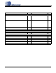
Hardware Mode Definitions
M0
M2
M3
17
16
15
42
Mode Selection (Input) - Determines the operational mode of the device as detailed in Table 6
and Table 7.
Soft ware Mode Definitions
SCL/CCLK 15
Serial Control Port Clock (Input) - Serial clock for the serial control port. Requires an external
pull-up resistor to the logic interface voltage in I²C
®
Mode as shown in the Typical Con nection
Diagram.
SDA/CDIN 16
Serial Control Port Dat a (Input/Output) - SDA is a data I/O line in I²C Mode and is open drain,
requiring an external pull-up resistor to the logic interface voltage, as shown in the Typical Con-
nection Diagram; CDIN is the input data line for the control po rt interface in SPI™ mode.
AD0/CS
17
Address Bit 0 (C) / Control Port Chip Select (SPI) (Input) - AD0 is a chip address pin in I²C
Mode; CS
is the chip select signal for SPI mode.
DSD Definitions
DSDA1
DSDB1
DSDA2
DSDB2
DSDA3
DSDB3
3
2
1
48
47
46
Direct Stream Digital Input (Input) - Input for Direct Stream Digital serial audio data.
DSD_SCLK 42 DSD Serial Clock (Input) - Serial clock for the Direct Stream Digital serial audio interface.
DSD_EN 7
DSD Enable (Input) - When held at logic ‘1’, the device will enter DSD Mode (Stand-Alone Mode
only).
Pin Name # Pin Description